

Effect of ribbon width on electrical transport properties of graphene nanoribbons
- PMID: 29577013
- PMCID: PMC5852198
- DOI: 10.1186/s40580-018-0139-0
Effect of ribbon width on electrical transport properties of graphene nanoribbons
Abstract
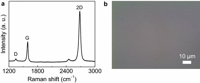
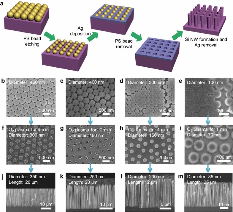
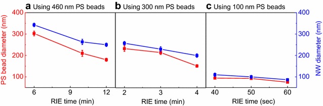
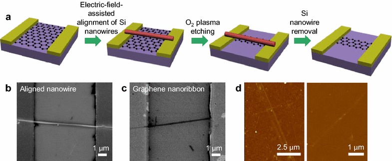
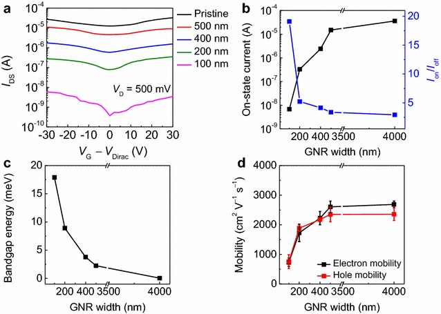
There has been growing interest in developing nanoelectronic devices based on graphene because of its superior electrical properties. In particular, patterning graphene into a nanoribbon can open a bandgap that can be tuned by changing the ribbon width, imparting semiconducting properties. In this study, we report the effect of ribbon width on electrical transport properties of graphene nanoribbons (GNRs). Monolayer graphene sheets and Si nanowires (NWs) were prepared by chemical vapor deposition and a combination of nanosphere lithography and metal-assisted electroless etching from a Si wafer, respectively. Back-gated GNR field-effect transistors were fabricated on a heavily p-doped Si substrate coated with a 300 nm-thick SiO2 layer, by O2 reactive ion etching of graphene sheets using etch masks based on Si NWs aligned on the graphene between the two electrodes by a dielectrophoresis method. This resulted in GNRs with various widths in a highly controllable manner, where the on/off current ratio was inversely proportional to ribbon width. The field-effect mobility decreased with decreasing GNR widths due to carrier scattering at the GNR edges. These results demonstrate the formation of a bandgap in GNRs due to enhanced carrier confinement in the transverse direction and edge effects when the GNR width is reduced.
Keywords: Electrical transport; Graphene; Graphene nanoribbon; Si nanowire.
Figures
Similar articles
-
Rational fabrication of graphene nanoribbons using a nanowire etch mask.Nano Lett. 2009 May;9(5):2083-7. doi: 10.1021/nl900531n. Nano Lett. 2009. PMID: 19344151
-
Patterning, characterization, and chemical sensing applications of graphene nanoribbon arrays down to 5 nm using helium ion beam lithography.ACS Nano. 2014 Feb 25;8(2):1538-46. doi: 10.1021/nn405759v. Epub 2014 Jan 27. ACS Nano. 2014. PMID: 24467172
-
Highly Aligned Polymeric Nanowire Etch-Mask Lithography Enabling the Integration of Graphene Nanoribbon Transistors.Nanomaterials (Basel). 2020 Dec 25;11(1):33. doi: 10.3390/nano11010033. Nanomaterials (Basel). 2020. PMID: 33375535 Free PMC article.
-
Modified Engineering of Graphene Nanoribbons Prepared via On-Surface Synthesis.Adv Mater. 2020 Feb;32(6):e1905957. doi: 10.1002/adma.201905957. Epub 2019 Dec 12. Adv Mater. 2020. PMID: 31830353 Review.
-
Graphene nanoribbon devices at high bias.Nano Converg. 2014;1(1):1. doi: 10.1186/s40580-014-0001-y. Epub 2014 Feb 20. Nano Converg. 2014. PMID: 28191387 Free PMC article. Review.
Cited by
-
Seeded growth of single-crystal black phosphorus nanoribbons.Nat Mater. 2024 Apr;23(4):470-478. doi: 10.1038/s41563-024-01830-2. Epub 2024 Feb 28. Nat Mater. 2024. PMID: 38418924
References
-
- Bolotin KI, Sikes KJ, Jiang Z, Klima M, Fudenberg G, Hone J, Kim P, Stormer HL. Solid State Commun. 2008;146:351. doi: 10.1016/j.ssc.2008.02.024. - DOI
LinkOut - more resources
Full Text Sources
Other Literature Sources