

Ridge Minimization of Ablated Morphologies on ITO Thin Films Using Squared Quasi-Flat Top Beam
- PMID: 29601515
- PMCID: PMC5951376
- DOI: 10.3390/ma11040530
Ridge Minimization of Ablated Morphologies on ITO Thin Films Using Squared Quasi-Flat Top Beam
Abstract
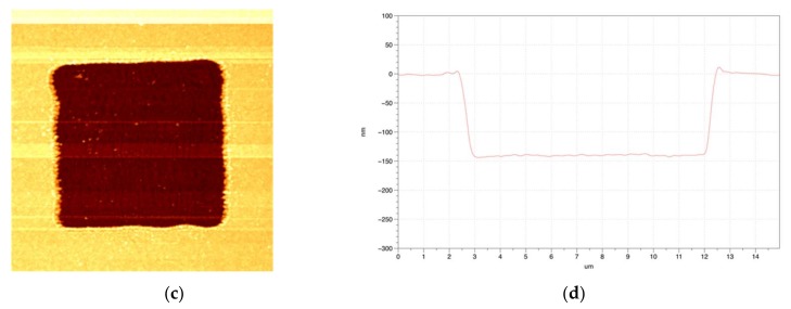
In this study, we explore the improvements in pattern quality that was obtained with a femtosecond laser with quasi-flat top beam profiles at the ablated edge of indium tin oxide (ITO) thin films for the patterning of optoelectronic devices. To ablate the ITO thin films, a femtosecond laser is used that has a wavelength and pulse duration of 1030 nm and 190 fs, respectively. The squared quasi-flat top beam is obtained from a circular Gaussian beam using slits with varying x-y axes. Then, the patterned ITO thin films are measured using both scanning electron and atomic force microscopes. In the case of the Gaussian beam, the ridge height and width are approximately 39 nm and 1.1 μm, respectively, whereas, when the quasi-flat top beam is used, the ridge height and width are approximately 7 nm and 0.25 μm, respectively.
Keywords: ITO thin film; ablation; femtosecond laser; ridge minimization; slit.
Conflict of interest statement
The authors declare no conflicts of interest.
Figures


References
-
- Trinh X.L., Duong T.H., Kim H.C. Large area controllable ITO patterning using micro-EDM and electrochemical etching. Int. J. Adv. Manuf. Technol. 2017;89:3681–3689. doi: 10.1007/s00170-016-9360-3. - DOI
-
- Cesaria M., Caricato A.P., Maruccio G., Martino M. Optical analysis of Cr-doped ITO films deposited by double-target laser ablation. J. Lumin. 2015;162:155–163. doi: 10.1016/j.jlumin.2015.02.047. - DOI
-
- Tseng S.F., Hsiao W.T., Huang K.C., Chiang D., Chen M.F., Chou C.P. Laserscribing of indium tin oxide (ITO) thin films deposited on various substrates for touch panels. Appl. Surf. Sci. 2010;257:1487–1494. doi: 10.1016/j.apsusc.2010.08.080. - DOI
-
- Li Z., Cho E.S., Kwon S.J. Laser direct patterning of the t-shaped ITO electrode for high-efficiency alternative current plasma display panels. Appl. Surf. Sci. 2010;257:776–780. doi: 10.1016/j.apsusc.2010.07.063. - DOI
LinkOut - more resources
Full Text Sources
Other Literature Sources
