. 2018 Apr 12;9(1):1417.
doi: 10.1038/s41467-018-03870-0.

Two-dimensional materials in functional three-dimensional architectures with applications in photodetection and imaging

Affiliations

Two-dimensional materials in functional three-dimensional architectures with applications in photodetection and imaging

Wonho Lee et al. Nat Commun. .

Abstract

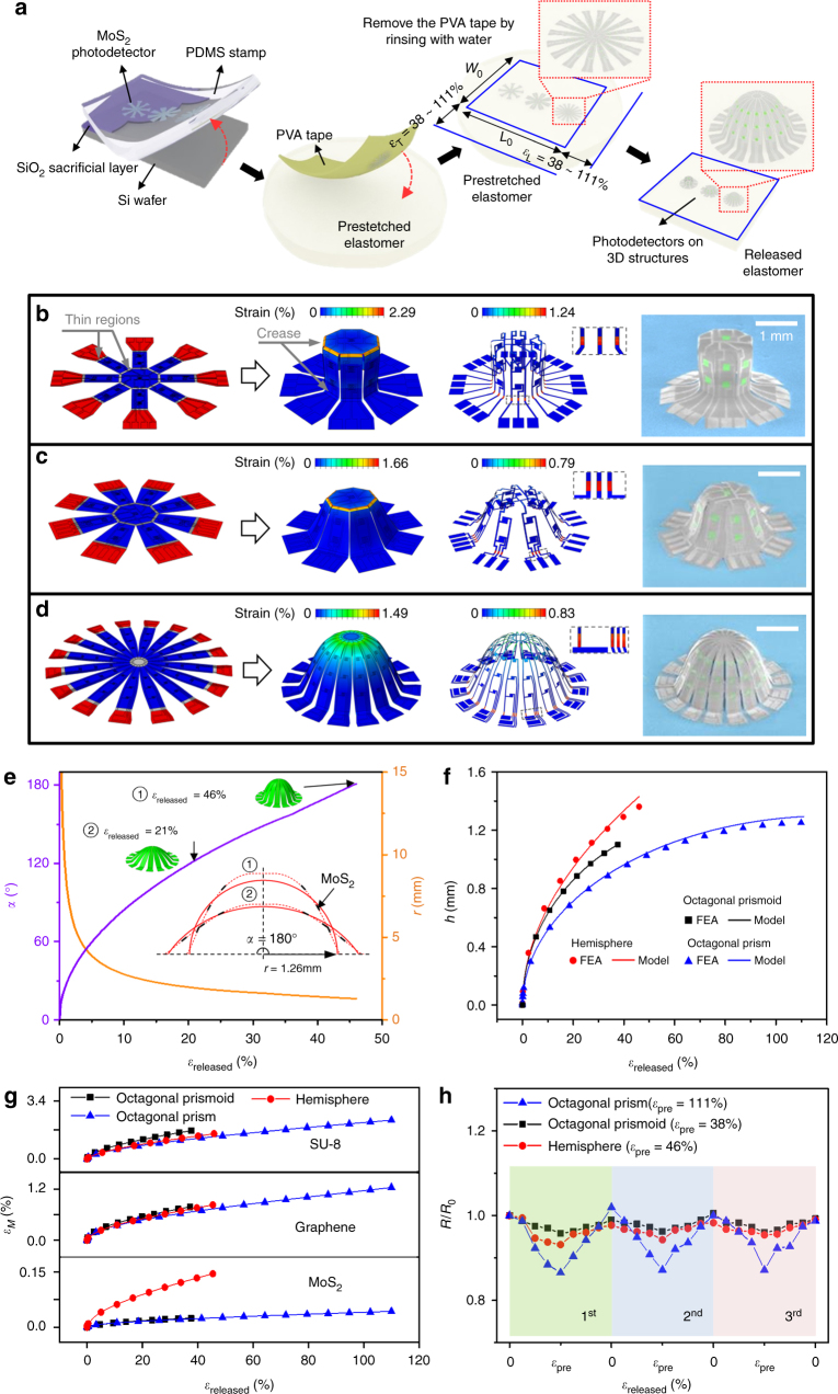
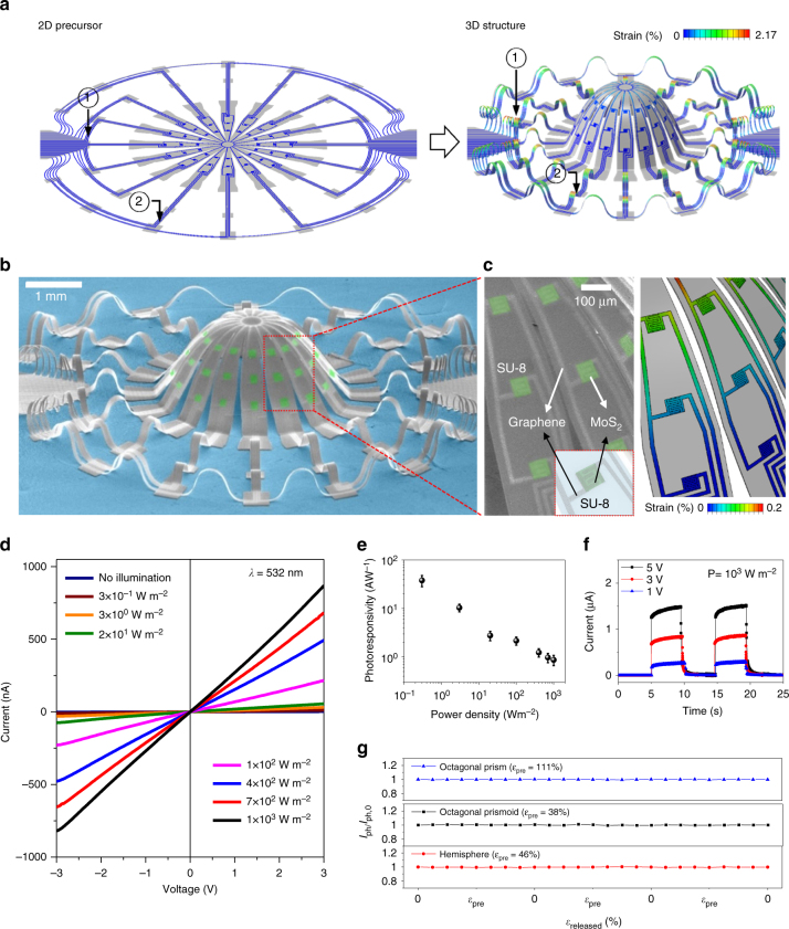
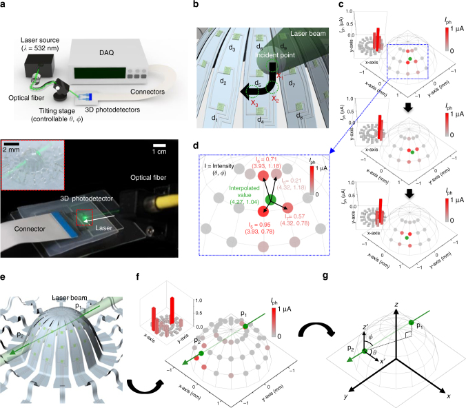
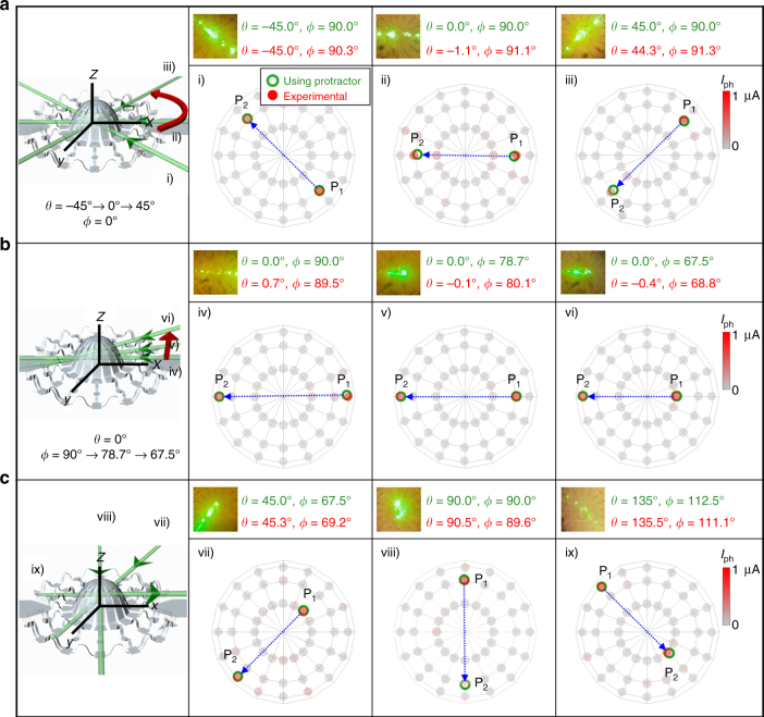
Efficient and highly functional three-dimensional systems that are ubiquitous in biology suggest that similar design architectures could be useful in electronic and optoelectronic technologies, extending their levels of functionality beyond those achievable with traditional, planar two-dimensional platforms. Complex three-dimensional structures inspired by origami, kirigami have promise as routes for two-dimensional to three-dimensional transformation, but current examples lack the necessary combination of functional materials, mechanics designs, system-level architectures, and integration capabilities for practical devices with unique operational features. Here, we show that two-dimensional semiconductor/semi-metal materials can play critical roles in this context, through demonstrations of complex, mechanically assembled three-dimensional systems for light-imaging capabilities that can encompass measurements of the direction, intensity and angular divergence properties of incident light. Specifically, the mechanics of graphene and MoS2, together with strategically configured supporting polymer films, can yield arrays of photodetectors in distinct, engineered three-dimensional geometries, including octagonal prisms, octagonal prismoids, and hemispherical domes.


Conflict of interest statement

The authors declare no competing interests.

Figures

Fig. 1
Fig. 1
Assembly and mechanical analysis of 3D photodetector structures from 2D materials. a Schematic illustration of processes for fabricating the 3D systems. b FEA results describing the formation of arrays of photodetectors based on graphene and MoS2 in the form of an octagonal prism, and corresponding colorized SEM images of the final configuration including MoS2 (green), graphene (light gray), and SU-8 (gray). c, d Similar FEA results for the cases of an octagonal prismoid and a hemisphere. Colors represent the magnitude of the maximum principal strain. e Central angle and radius of a cross-section of the hemisphere in d vs. the released pre-strain. Here, the insets denote an intermediate state (εreleased = 21.4%) and the final state (εreleased = 46%) of pre-strain release, with the dashed and solid lines representing the profiles from FEA and fitting arcs, respectively. f FEA results and analytic predictions of the height of three photodetector structures in bd. g Computational study of tensile strain applied to the SU-8, graphene, and MoS2 layers vs. pre-strain during the 3D assembly (squares, circles, and triangles denote the octagonal frustum, hemisphere, and octagonal prism, respectively). h Experimentally measured variation in the resistance in graphene during repeated buckling processes
Fig. 2
Fig. 2
Interconnect design and photoinduced response of MoS2 photodetectors on a 3D hemispherical structure. a FEA of the 3D hemisphere structures before and after compressive buckling, showing the distributions of maximum principal strains in the MoS2 photodetectors and 3D interconnects. b Colorized SEM image of MoS2 photodetectors consisting of MoS2 (green), graphene (light gray), and SU-8 (gray) on the hemisphere with 3D interconnects. c Magnified view of the SEM image in b and corresponding FEA results for the strain distribution. Inset: schematic illustration of the unit device enclosed by the red box in the main image. d IV characteristics of the 3D photodetector at different bias voltages (laser-beam wavelength = 532 nm, power density = 1000 W m−2). e Photoresponsivity of the MoS2 photodetector at a bias voltage of 3 V for different laser power densities. (Standard deviation of 48 sampling distribution recorded from 48 devices.) f Time-resolved photoresponses of the devices under laser illumination at different power densities. g Variation in photocurrent during repeated buckling processes for the octagonal prism (top), octagonal prismoid (middle), and hemispherical structure (bottom)
Fig. 3
Fig. 3
Operating principles of a 3D photodetection and imaging system. a Schematic illustration and optical images of the system. Inset: magnified view. b Distribution of the devices and movement of the laser beam. c Photocurrent distribution on the hemisphere surface during movement of the laser beam. d Magnified view of the photocurrent distribution at the first position of the laser beam. The illuminating locations of the incident laser beam are estimated by interpolation. e Penetration of the laser beam at two points of the 3D hemispherical surface. f Photocurrent distribution on the hemisphere surface in the scenario of e. g Principle of estimating the incident direction of the laser from the photocurrent map
Fig. 4
Fig. 4
Sensing characteristics of a 3D photodetection and imaging system. a Maps of photocurrent measured across the 3D surfaces. The incident angle θ ranges from −45° to 45° with φ fixed at 90°. The measured θ and φ from the device arrays are shown for comparison. b Similar results with φ ranging from 90° to 67.5° and θ = 0°. c Photocurrent maps of the photodetector array on the 3D surfaces randomly penetrated at two points by the incident laser. The incident angles are (from left to right) θ = 45°, φ = 67.5°, θ = 90°, φ = 90°, and θ = 135°, φ = 112.5°

References

    1. Soukoulis CM, Wegener M. Past achievements and future challenges in the development of three-dimensional photonic metamaterials. Nat. Photon. 2011;5:523–530. doi: 10.1038/nphoton.2011.154. - DOI
    1. Douglas SM, et al. Self-assembly of DNA into nanoscale three-dimensional shapes. Nature. 2009;459:414–418. doi: 10.1038/nature08016. - DOI - PMC - PubMed
    1. Zhang H, Yu X, Braun PV. Three-dimensional bicontinuous ultrafast-charge and -discharge bulk battery electrodes. Nat. Nanotechnol. 2011;6:277–281. doi: 10.1038/nnano.2011.38. - DOI - PubMed
    1. Wegst UG, Bai H, Saiz E, Tomsia AP, Ritchie RO. Bioinspired structural materials. Nat. Mater. 2015;14:23–36. doi: 10.1038/nmat4089. - DOI - PubMed
    1. Shenoy VB, Gracias DH. Self-folding thin-film materials: from nanopolyhedra to graphene origami. MRS Bull. 2012;37:847–854. doi: 10.1557/mrs.2012.184. - DOI

Publication types