. 2018 Apr 23;8(1):6381.
doi: 10.1038/s41598-018-23922-1.

Quantitative optical mapping of two-dimensional materials

Affiliations

Quantitative optical mapping of two-dimensional materials

Bjarke S Jessen et al. Sci Rep. .

Abstract

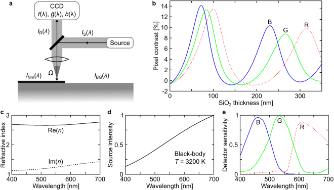
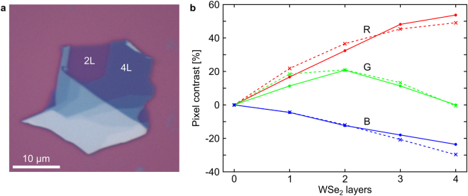
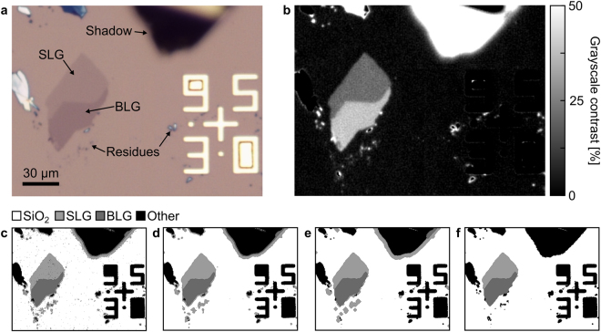
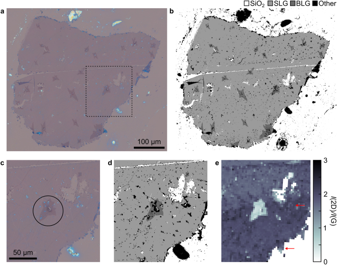
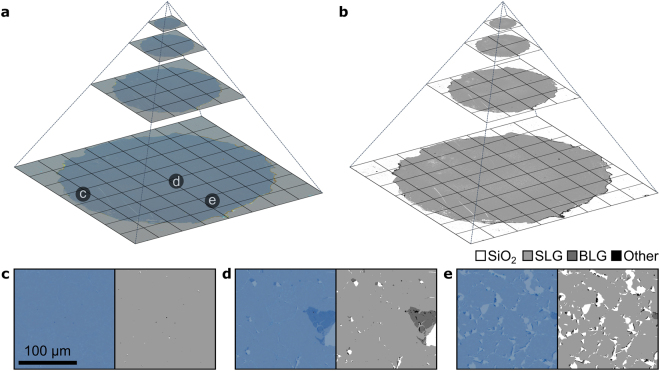
The pace of two-dimensional materials (2DM) research has been greatly accelerated by the ability to identify exfoliated thicknesses down to a monolayer from their optical contrast. Since this process requires time-consuming and error-prone manual assignment to avoid false-positives from image features with similar contrast, efforts towards fast and reliable automated assignments schemes is essential. We show that by modelling the expected 2DM contrast in digitally captured images, we can automatically identify candidate regions of 2DM. More importantly, we show a computationally-light machine vision strategy for eliminating false-positives from this set of 2DM candidates through the combined use of binary thresholding, opening and closing filters, and shape-analysis from edge detection. Calculation of data pyramids for arbitrarily high-resolution optical coverage maps of two-dimensional materials produced in this way allows the real-time presentation and processing of this image data in a zoomable interface, enabling large datasets to be explored and analysed with ease. The result is that a standard optical microscope with CCD camera can be used as an analysis tool able to accurately determine the coverage, residue/contamination concentration, and layer number for a wide range of presented 2DMs.


Conflict of interest statement

The authors declare no competing interests.

Figures

Figure 1
Figure 1
(a) Illustration of a typical optical setup where light from a source with spectral intensity IS(λ) interacts with the substrate and optical components and arrives at a detector as IR(λ). Ifilm(λ) and IBG(λ) are the reflected spectral intensities from the material to be identified and the background, respectively. (b) Calculated red, green and blue pixel contrast of single-layer graphene on a SiO2/Si substrate as a function of varying thickness of SiO2. (c,d,e) Wavelength-dependent input to the contrast calculations. (c) Real and imaginary part of the refractive index of graphene. (d) Typical intensity characteristics of an incandescent light-source. (e) Spectral sensitivity of a Sony ICX282AQ CCD camera.
Figure 2
Figure 2
(a) Optical image of exfoliated WSe2 crystal with different number of layers on 300 nm SiO2. (b) Contrast of WSe2 as a function of number of layers on 300 nm SiO2. Crosses are calculated contrasts based on the wavelength dependent refractive index of WSe2. Dots are extracted from digital optical images with red, green and blue channels giving three separate values of contrasts for each thickness.
Figure 3
Figure 3
(a) Optical image of exfoliated graphene on 300 nm SiO2. The sample contains typical features of an optical image of an exfoliated sample, such as single- and bi-layer graphene, graphite, and residues, a shadow from bulk graphite, and optical alignment marks. (b) Map of the positive grey-scale contrasts in the image. (c) Segmented image where every pixel has been categorized either as SLG, BLG, SiO2, or other, using only the expected contrast values. (d) Segmented image after edge-preserving median filtering, and (e) after erode and dilate filtering. (f) Segmented image after contour filtering, resulting in a >99% pixel-for-pixel correspondence between expected and automatically detected pixels.
Figure 4
Figure 4
Comparison between optical, coverage and Raman maps of CVD graphene transferred by wet etching to 90 nm SiO2. (a) Optical map of graphene consisting of several images stitched together. (b) Coverage map of the sample in (a) with colour codes for SiO2, SLG, BLG, and other. (c) Zoom-in on the area inside the dotted square in (a) with the corresponding coverage map in (d) showing the detail level of the optical and coverage maps. The circle in (a) highlights an area with BLG surrounding a small region with three layer graphene and SiO2. (e) Raman map of the I(2D)/I(G) peak intensity ratio for the area shown in (c) and (d).
Figure 5
Figure 5
(a) Representation of the data-pyramid of a 12 mm wide circular sample of CVD graphene transferred to 90 nm SiO2 using oxidative decoupling transfer, while (b) is the corresponding data pyramid from coverage analysis. The contrast of images is slightly enhanced to increase visibility. In the left and right sides of figure (ce) is shown the raw images and digitally detected counterparts, respectively, of selected areas in the data-pyramid highlighted in (a). The dataset is 16·109 (16 giga) RGB pixels.

References

    1. Blake P, et al. Making graphene visible. Appl. Phys. Lett. 2007;91:63124. doi: 10.1063/1.2768624. - DOI
    1. Gorbachev RV, et al. Hunting for monolayer boron nitride: Optical and raman signatures. Small. 2011;7:465–468. doi: 10.1002/smll.201001628. - DOI - PubMed
    1. Pizzocchero F, et al. Non-destructive electrochemical graphene transfer from reusable thin-film catalysts. Carbon. 2015;85:397–405. doi: 10.1016/j.carbon.2014.12.061. - DOI
    1. Whelan PR, et al. Raman spectral indicators of catalyst decoupling for transfer of CVD grown 2D materials. Carbon. 2017;117:75–81. doi: 10.1016/j.carbon.2017.02.028. - DOI
    1. Wang R, et al. ACS Appl. Mater. Interfaces. 2016. Catalyst interface engineering for improved 2D film lift-off and transfer; pp. 33072–33082. - PMC - PubMed

Publication types

LinkOut - more resources