. 2018 Apr 24;9(1):1625.
doi: 10.1038/s41467-018-04028-8.

Molecular doping enabled scalable blading of efficient hole-transport-layer-free perovskite solar cells

Affiliations

Molecular doping enabled scalable blading of efficient hole-transport-layer-free perovskite solar cells

Wu-Qiang Wu et al. Nat Commun. .

Abstract

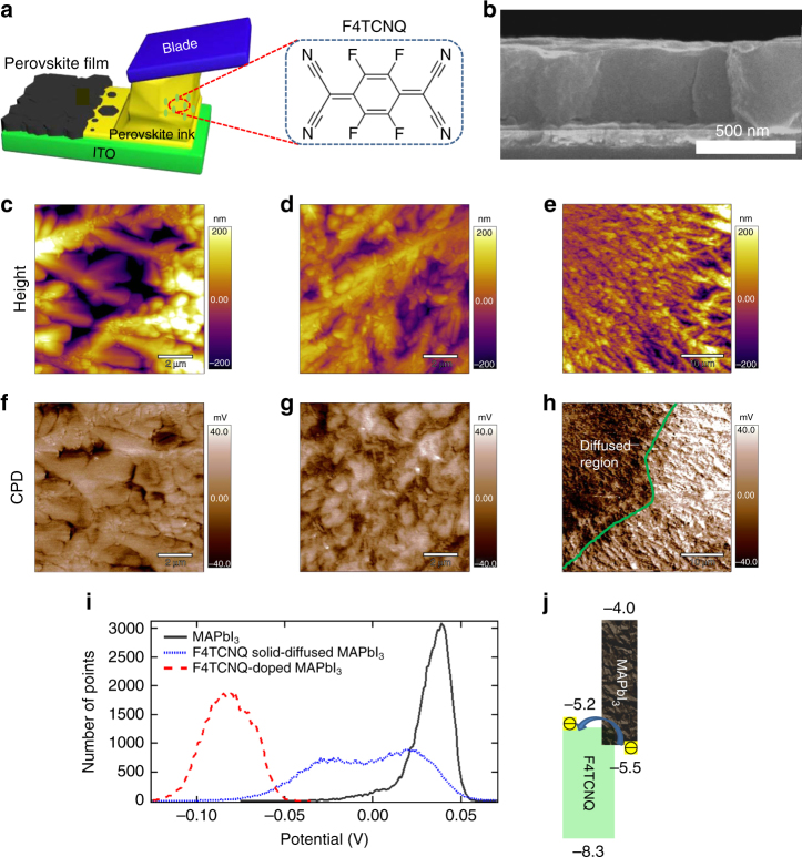
The efficiencies of perovskite solar cells (PSCs) are now reaching such consistently high levels that scalable manufacturing at low cost is becoming critical. However, this remains challenging due to the expensive hole-transporting materials usually employed, and difficulties associated with the scalable deposition of other functional layers. By simplifying the device architecture, hole-transport-layer-free PSCs with improved photovoltaic performance are fabricated via a scalable doctor-blading process. Molecular doping of halide perovskite films improved the conductivity of the films and their electronic contact with the conductive substrate, resulting in a reduced series resistance. It facilitates the extraction of photoexcited holes from perovskite directly to the conductive substrate. The bladed hole-transport-layer-free PSCs showed a stabilized power conversion efficiency above 20.0%. This work represents a significant step towards the scalable, cost-effective manufacturing of PSCs with both high performance and simple fabrication processes.


Conflict of interest statement

The authors declare no competing interests.

Figures

Fig. 1
Fig. 1
Doctor blading and doping of perovskite films by F4TCNQ. a Schematic illustration of a doctor-bladed perovskite film and the chemical structure of F4TCNQ dopant. b Cross-sectional SEM image of the MAPbI3 film deposited directly onto ITO glass via bladed coating at 150 °C, showing the film thickness of around 500 nm. Topography KPFM images of c, f MAPbI3, d, g F4TCNQ-doped MAPbI3, and e, h F4TCNQ solid-diffused MAPbI3 films. CPD represents the contact potential difference between the tip and sample’s surface. i Surface potential profiles of different perovskite films as indicated. j Schematic illustration of the energy diagram and electron transfer process for MAPbI3:F4TCNQ blends
Fig. 2
Fig. 2
Conductivities and photoluminescence lifetimes of neat or doped perovskite films. a Geometry for the lateral conductivity measurement: the perovskite films were 500 nm thick, with 1 mm gold (Au) electrodes separated by 100 μm. b J–V curves of neat or F4TCNQ-doped MAPbI3 deposited on normal glass substrates, where the current was measured along the lateral direction. c TRPL decay curves of glass/MAPbI3 and glass/MAPbI3:F4TCNQ. PL lifetimes were calculated by single exponential fitting. d c-AFM setup. Topographic AFM images of e MAPbI3 and g MAPbI3:F4TCNQ films, with locations where the c-AFM tip measured the grain and GB currents. Local dark currents measured at the GBs and on the grains for the f MAPbI3 film and h MAPbI3:F4TCNQ film
Fig. 3
Fig. 3
Perovskite film morphology, device structure, and photovoltaic performance. a Low magnification and b high magnification SEM images of bladed and doped MAPbI3 film prepared with MHP (0.225 wt%) and MACl (0.5 wt%) as additive, followed by co-solvents annealing treatment. c Schematic illustration of the HTL-free device configuration. d J–V characteristics, e Steady-state current and stabilized PCE measured at a maximum power point (0.93 V), f EQE and integrated current density, and g PCE histogram of PSCs based on MAPbI3:F4TCNQ films (with 0.03 wt% F4TCNQ)
Fig. 4
Fig. 4
Interfacial hole transfer dynamics. Schematic illustrations of hole transfer at the a ITO/MAPbI3 or b ITO/F4TCNQ-doped MAPbI3 interface

References

    1. Kojima A, Teshima K, Shirai Y, Miyasaka T. Organometal halide perovskites as visible-light sensitizers for photovoltaic cells. J. Am. Chem. Soc. 2009;131:6050–6051. doi: 10.1021/ja809598r. - DOI - PubMed
    1. Correa-Baena JP, et al. The rapid evolution of highly efficient perovskite solar cells. Energy Environ. Sci. 2017;10:710–727. doi: 10.1039/C6EE03397K. - DOI
    1. Li X, et al. A vacuum flash–assisted solution process for high-efficiency large-area perovskite solar cells. Science. 2016;353:58–62. doi: 10.1126/science.aaf8060. - DOI - PubMed
    1. Yang WS, et al. Iodide management in formamidinium-lead-halide–based perovskite layers for efficient solar cells. Science. 2017;356:1376–1379. doi: 10.1126/science.aan2301. - DOI - PubMed
    1. Zheng X, et al. Defect passivation in hybrid perovskite solar cells using quaternary ammonium halide anions and cations. Nat. Energy. 2017;2:17102. doi: 10.1038/nenergy.2017.102. - DOI

Publication types