. 2018 Apr;556(7702):483-486.
doi: 10.1038/s41586-018-0031-4. Epub 2018 Apr 25.

Low-loss plasmon-assisted electro-optic modulator

Affiliations

Low-loss plasmon-assisted electro-optic modulator

Christian Haffner et al. Nature. 2018 Apr.

Abstract

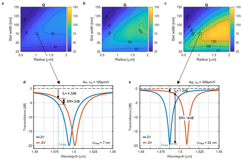
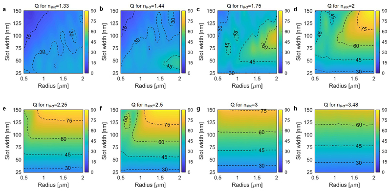
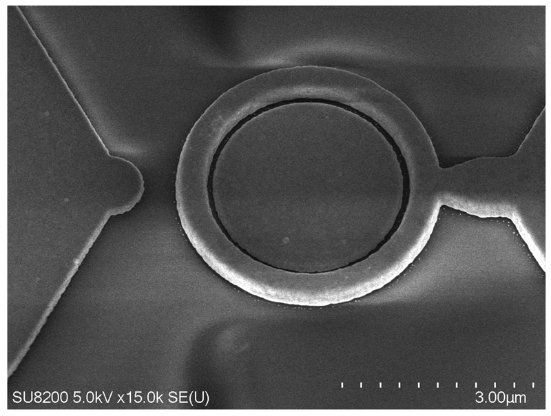
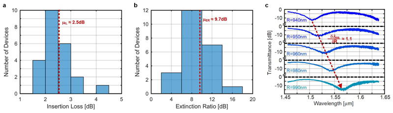
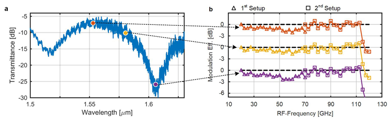
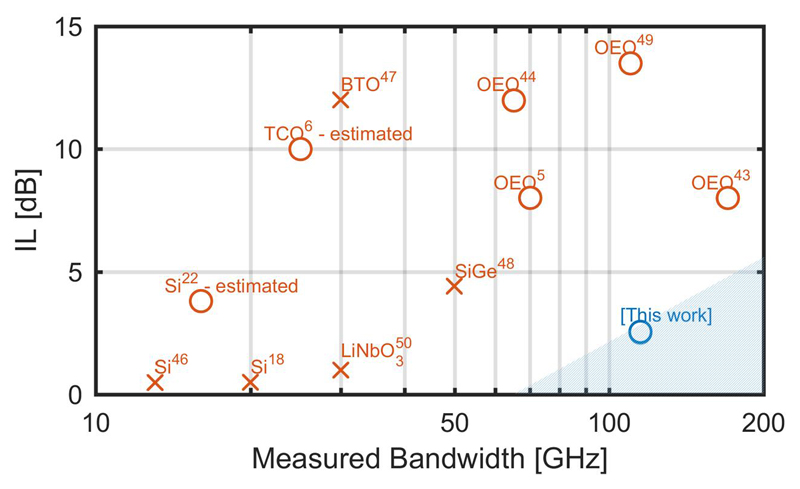
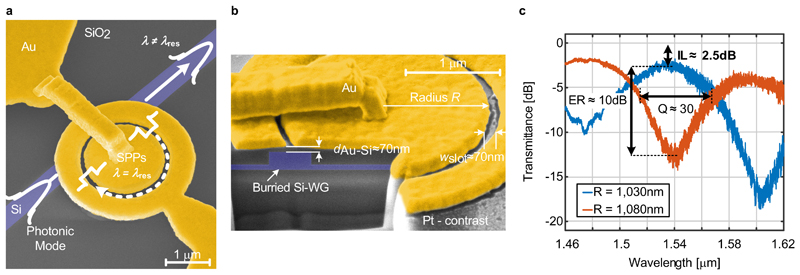
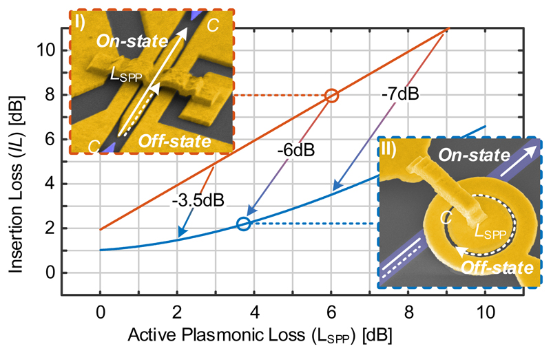
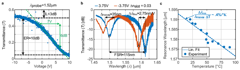
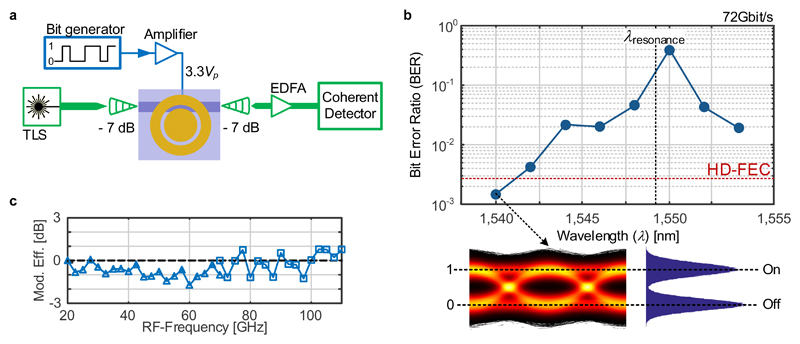
For nearly two decades, researchers in the field of plasmonics 1 -which studies the coupling of electromagnetic waves to the motion of free electrons near the surface of a metal 2 -have sought to realize subwavelength optical devices for information technology3-6, sensing7,8, nonlinear optics9,10, optical nanotweezers 11 and biomedical applications 12 . However, the electron motion generates heat through ohmic losses. Although this heat is desirable for some applications such as photo-thermal therapy, it is a disadvantage in plasmonic devices for sensing and information technology 13 and has led to a widespread view that plasmonics is too lossy to be practical. Here we demonstrate that the ohmic losses can be bypassed by using 'resonant switching'. In the proposed approach, light is coupled to the lossy surface plasmon polaritons only in the device's off state (in resonance) in which attenuation is desired, to ensure large extinction ratios between the on and off states and allow subpicosecond switching. In the on state (out of resonance), destructive interference prevents the light from coupling to the lossy plasmonic section of a device. To validate the approach, we fabricated a plasmonic electro-optic ring modulator. The experiments confirm that low on-chip optical losses, operation at over 100 gigahertz, good energy efficiency, low thermal drift and a compact footprint can be combined in a single device. Our result illustrates that plasmonics has the potential to enable fast, compact on-chip sensing and communications technologies.


Conflict of interest statement

No author has a competing financial interest.

Figures

Extended Data Figure 1
Resonator performance for various plasmonic materials. (a) Gold (Au) which is interesting for research due to its chemical stability. (b) Copper (Cu) is of interest as it is a CMOS-compatible material. (c) Silver (Ag) feature the best plasmonic properties and could be of interest for high performance applications. Switching capability of an (d) gold and (e) silver ring resonator for a 2V bias The latter utilizes the newest OEO material, which has a three-times-larger electro-optic coefficient r33. The performance improvement enables a significant reduction in terms of the driving voltage. The number at the bottom right indicates the shift in the resonance wavelength.
Extended Data Figure 2
Q-factors of various materials filling the slot. The materials differ in their refractive index and one can observe that low n-materials are limited by bending loss (diagonal lines) while high n-materials are limited by propagation loss (parallel lines). Please note these simulations were performed with 150 nm height of the outer and inner electrode to account for limitations in fabrication processes different to ours.
Extended Data Figure 3
Tilted SEM image of a processed ring resonator. The different height of the outer and inner electrodes reduces the bending losses.
Extended Data Figure 4
Reproducibility of plasmonic ring resonators. Insertion loss (a) and extinction ratio (b) histograms. Data are obtained from passive measurements of 23 devices with a designed slot with of 80 nm and radii ranging from 900 nm to 1100 nm. (c) Dependence of the resonance wavelength versus ring radius.
Extended Data Figure 5
Transmission spectrum (a) and the measured bandwidth (b) at the off-resonance, 3dB and on-resonance operating point. No bandwidth limitation can be observed up to 110 GHz. The drop at 115 Ghz frequencies is due to a limited measurement setup. Recent studies show that the modulation efficiency at lower RF-frequency is not limited44
Extended Data Figure 6
Technology overview in terms of insertion loss and bandwidth of electro-optic modulators. Ideal Candidates should feature low insertion loss with high electro-optic (EO) bandwidths found.
Figure 1
Figure 1
False-colored SEM image of a plasmonic ring resonator and the corresponding transmittance over wavelength. (a) Top view and (b) cross section of the resonator. Photonic modes propagating in the buried silicon waveguide resonator couple partially to the SPPs in the metal-insulator-metal-ring when the resonance condition is fulfilled. While out of resonance operation results in a low loss light transmission. (c) Passive measurements of two identical ring resonators that only differ in radii (blue - 1030 nm; red - 1080 nm). Due to the resonant approach, insertion losses of 2.5 dB are measured with extinction ratios (ER) above 10 dB.
Figure 2
Figure 2
Theoretical loss advantage of critical coupled resonant over non-resonant push-pull Mach-Zehnder devices. The IL are plotted over the active plasmonic loss (LSPP) in the slot waveguide of the MZ (left inset, red) and resonator (right inset, blue). Losses can be reduced by more than 6 dB. This is due to following reasons: I) bypassing mechanism – only a fraction of light experiences plasmonic losses; II) resonant enhancement – resonators achieve the same modulation depth for shorter devices than their non-resonant counterpart (indicated by the arrows); and III) coupling scheme – non-resonant approaches require two photonic/SPP converters while resonant approaches require only one.
Figure 3
Figure 3
Sensitivity and stability of the plasmonic resonator. (a) Voltage sensitivity of the resonator’s transmittance. (b) Sensitivity of the ring as a function of the wavelength. A change (Δnslot≈0.03) in the refractive index of the slot-filling material causes a large change of the resonance wavelength (blue/red). (c) The resonator shows stable operation across a large thermal variation. These characteristics make the plasmonic MIM-ring resonator a promising candidate in the field of optical modulators and sensors.
Figure 4
Figure 4
High-speed data experiments with a plasmonic ring resonator used as an EO-modulator. (a) Depicts the experimental setup. (b) Bit-error-ratio (BER) vs. wavelength for a resonator with λresonance = 1549nm. BERs below the hard-decision forward error correction (HD-FEC) limit show successful data modulation and detection without the use of a temperature control. The BER increases at the resonance wavelength as expected from the notch-filter response of the resonator. (c) Shows the bandwidth of the plasmonic resonator in the bottom, which is beyond 110 GHz.

References

    1. Maier SA, et al. Plasmonics—A Route to Nanoscale Optical Devices. Advanced Materials. 2001;13:1501–1505.
    1. Gramotnev DK, Bozhevolnyi SI. Plasmonics beyond the diffraction limit. Nat Photonics. 2010;4:83–91. doi: 10.1038/nphoton.2009.282. - DOI
    1. Dionne JA, Diest K, Sweatlock LA, Atwater HA. PlasMOStor: A Metal–Oxide–Si Field Effect Plasmonic Modulator. Nano Letters. 2009;9:897–902. doi: 10.1021/nl803868k. - DOI - PubMed
    1. Sorger VJ, Lanzillotti-Kimura Norberto D, Ma R-M, Zhang X. Ultra-compact silicon nanophotonic modulator with broadband response. Nanophotonics. 2012;1:17. doi: 10.1515/nanoph-2012-0009. - DOI
    1. Haffner C, et al. All-plasmonic Mach–Zehnder modulator enabling optical high-speed communication at the microscale. Nat Photon. 2015;9:525–528.

Publication types