. 2018 May 2;9(1):1768.
doi: 10.1038/s41467-018-04200-0.

A silicon metal-oxide-semiconductor electron spin-orbit qubit

Affiliations

A silicon metal-oxide-semiconductor electron spin-orbit qubit

Ryan M Jock et al. Nat Commun. .

Abstract

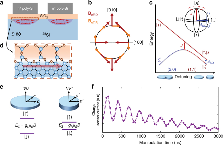
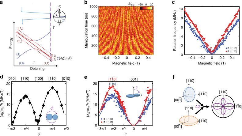
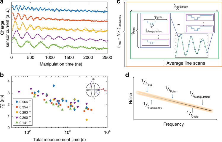
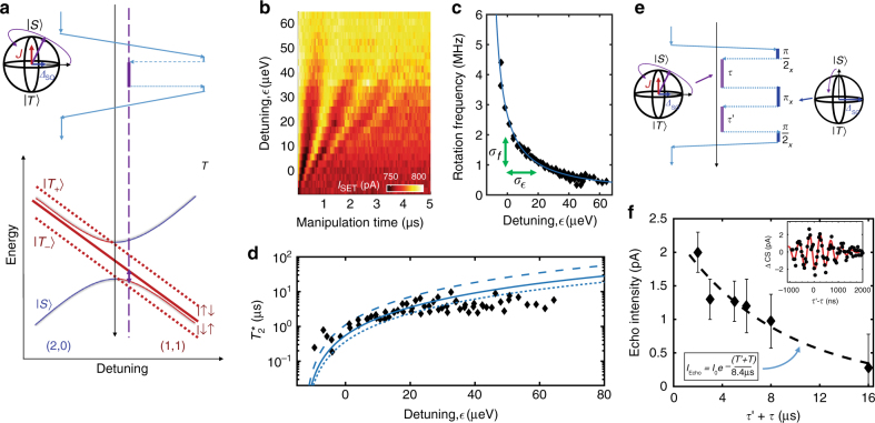
The silicon metal-oxide-semiconductor (MOS) material system is a technologically important implementation of spin-based quantum information processing. However, the MOS interface is imperfect leading to concerns about 1/f trap noise and variability in the electron g-factor due to spin-orbit (SO) effects. Here we advantageously use interface-SO coupling for a critical control axis in a double-quantum-dot singlet-triplet qubit. The magnetic field-orientation dependence of the g-factors is consistent with Rashba and Dresselhaus interface-SO contributions. The resulting all-electrical, two-axis control is also used to probe the MOS interface noise. The measured inhomogeneous dephasing time, [Formula: see text], of 1.6 μs is consistent with 99.95% 28Si enrichment. Furthermore, when tuned to be sensitive to exchange fluctuations, a quasi-static charge noise detuning variance of 2 μeV is observed, competitive with low-noise reports in other semiconductor qubits. This work, therefore, demonstrates that the MOS interface inherently provides properties for two-axis qubit control, while not increasing noise relative to other material choices.


Conflict of interest statement

The authors declare no competing interests.

Figures

Fig. 1
Fig. 1
MOS spin–orbit-driven singlet–triplet qubit. a Cartoon representation of the interface spin–orbit interaction. For an electron confined to a QD, an in-plane magnetic field will cause a finite momentum at the interface which, in the presence of broken inversion symmetry, leads to a spin–orbit interaction. The position of the QDs presented in this work, relative to the gates, differs from what is portrayed here (see Supplementary Fig. 2). b Schematic example of the effective spin–orbit field due to the Dresselhaus (red) and Rashba (orange) interactions for in-plane electron momentum. c Schematic energy diagram of the DQD near the (2, 0) → (1, 1) charge transition, showing the energy of the singlet and triplet states as a function of QD–QD detuning, ϵ. Near the interdot transition (ϵ = 0), the exchange energy, J, dominates the electronic interaction and drives rotations about the Z-axis (red arrow in inset). Deep into the (1, 1) charge sector (ϵ > 0), J is small and the electronic states rotate about the X-axis due to a difference in Zeeman energy between each QD (blue arrow in inset). d Details of the interface at the inter-atomic bond level govern the spin–orbit interaction. e The local electrostatic environment of each QD leads to different momenta and electric fields at the interface and, thus, distinct spin–orbit interactions and Zeeman energy splitting. f Charge sensor current as a function of time spent deep in the (1, 1) charge sector, where higher current indicates a higher probability of measuring a singlet state. The oscillations indicate clear X-rotations due to a difference in spin–orbit interaction in each QD
Fig. 2
Fig. 2
MOS interface spin–orbit interaction. a Energy diagram and gate pulse schematic for controlling spin–orbit rotations. We initialize the qubit into the S(2, 0) ground state and transfer the system to the (1, 1) charge sector with a rapid adiabatic pulse, such that it remains a singlet. The difference in Zeeman splitting between the QDs drives X-rotations between the S(1, 1) and T0(1, 1) states. A rapid adiabatic return pulse projects the states onto the S(2, 0) and T0(1, 1) basis for measurement. b Change in charge sensor current as a function of X-rotation manipulation time as the magnetic field is varied along the [11¯0] crystallographic direction. c The extracted rotation frequency as a function of magnetic field strength along the [110] and [11¯0] crystallographic directions. d, e Magnetic field angular dependence of the SO-driven difference in g-factor between the dots for the in-plane, θ, and out-of-plane, ϕ, directions, respectively. Fits to the form (Δg)μBBh = BΔα-Δβsin(2ϕ) sin2(θ) are also plotted for θ = π/2 (black), ϕ = 3π/4 (blue) and ϕ = π/4 (red). f A cartoon representation of the angular dependence of the two QDs (left). The difference between the QD g-factors give an in-plane dependence represented by the cloverleaf plot on the right
Fig. 3
Fig. 3
Measurement time dependence. a Long-time (50 min) averaged measurements of singlet return signal as a function of manipulation time for several magnetic field strengths aligned along the [11¯0] crystallographic direction. The data for each field has been shifted for clarity. b The extracted T2 as a function of total experimental measurement time. (inset) Magnetic noise creates fluctuations in the effective magnetic field at each QD, leading to variation in the X-rotation frequency throughout the measurement. c Relevant time scales of the measurement. The shortest time scale susceptible to noise in the experiment is the time spent manipulating the qubit. In the limit of quasi-static noise, we expect the qubit to have a constant environment during this time. However, over the course of a total pulse cycle (which consists of qubit preparation and measurement and may be several ms in length), the environment may change. Furthermore, as the cycle is repeated and averaged by the lock-in for each data point, each data point is collected for a free induction decay curve. As successive curves are averaged together, the distribution of noise that is sampled grows larger. d During the course of the measurement, the qubit is susceptible to noise in the frequency band between 1/tTotal and 1/tManipulation
Fig. 4
Fig. 4
Z-rotations and noise. a Energy Diagram and gate pulse schematic for controlling exchange rotations. We initialize the qubit into the S(2, 0) ground state and ramp adiabatically, such that it transfers to the ground in the (1, 1) charge sector. A fast pulse to and from a detuning, ϵ, where J is substantial drives coherent rotations around an axis depending on both J and ΔSO. Returning to the (2, 0) charge sector adiabatically projects the states onto the S(2, 0) and T0(1, 1) basis for measurement. b Measured charge sensor current as a function of the time spent rotating for various detuning points. Here, high current corresponds to a higher probability of measuring a singlet. c The extracted rotation frequency vs. detuning. The blue line is a fit to the form J(ϵ)2+ΔSO2, where J(ϵ) ∝ ϵ−1. d Extracted T2 as a function of detuning. We also plot the long integration time values from Fig. 3a. The blue lines are fits to the form T2 = 12πσedfdϵ-1, where the extracted charge noise, σϵ, is 1 (dashed), 2 (solid) and 3 μeV (dotted). e Gate pulse schematic for a Hahn-echo sequence. We initialize the qubit into the S(2, 0) ground state and transfer the system to the (1, 1) charge sector with a rapid adiabatic pulse such that it remains in a singlet state. Combinations of ΔSO-rotations about the X-axis and J-rotations about a second axis provide access to entire Bloch sphere. This echo sequence counteracts low frequency noise, prolonging qubit coherence. f Hahn-echo amplitude as a function of total time, τ′ + τ, exposed to charge noise at detuning ϵ. The error bars represent 95% confidence interval. A fit to an exponential decay gives qubit coherence time of T2eecho = 8.4 μs. (inset) Measured echo signal for τ = 1 μs with B = 0.141 T along the [110] direction. The change in charge sensor current (ΔCS) due to the echo signal has an oscillation frequency corresponding to ΔSO and a Gaussian envelope around τ = τ′ with a decay due to the inhomogeneous dephasing time of T2e* = 1 μs

References

    1. Tyryshkin AM, et al. Electron spin coherence exceeding seconds in high-purity silicon. Nat. Mater. 2012;11:143–147. doi: 10.1038/nmat3182. - DOI - PubMed
    1. Veldhorst M, et al. An addressable quantum dot qubit with fault-tolerant control-fidelity. Nat. Nano. 2014;9:981–985. doi: 10.1038/nnano.2014.216. - DOI - PubMed
    1. Veldhorst M, et al. A two-qubit logic gate in silicon. Nature. 2015;526:410–414. doi: 10.1038/nature15263. - DOI - PubMed
    1. Gamble JK, et al. Valley splitting of single-electron Si MOS quantum dots. Appl. Phys. Lett. 2016;109:253101. doi: 10.1063/1.4972514. - DOI
    1. Rochette, S. et al. Single-electron-occupation metal-oxide-semiconductor quantum dots formed from efficient poly-silicon gate layout. Preprint at http://arxiv.org/abs/1707.03895 (2017).Ne

Publication types