Development of Ordered, Porous (Sub-25 nm Dimensions) Surface Membrane Structures Using a Block Copolymer Approach
- PMID: 29740003
- PMCID: PMC5940818
- DOI: 10.1038/s41598-018-25446-0
Development of Ordered, Porous (Sub-25 nm Dimensions) Surface Membrane Structures Using a Block Copolymer Approach
Abstract
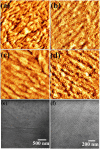
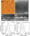
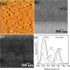
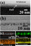
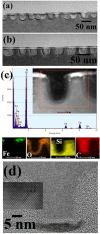
In an effort to develop block copolymer lithography to create high aspect vertical pore arrangements in a substrate surface we have used a microphase separated poly(ethylene oxide) -b- polystyrene (PEO-b-PS) block copolymer (BCP) thin film where (and most unusually) PS not PEO is the cylinder forming phase and PEO is the majority block. Compared to previous work, we can amplify etch contrast by inclusion of hard mask material into the matrix block allowing the cylinder polymer to be removed and the exposed substrate subject to deep etching thereby generating uniform, arranged, sub-25 nm cylindrical nanopore arrays. Briefly, selective metal ion inclusion into the PEO matrix and subsequent processing (etch/modification) was applied for creating iron oxide nanohole arrays. The oxide nanoholes (22 nm diameter) were cylindrical, uniform diameter and mimics the original BCP nanopatterns. The oxide nanohole network is demonstrated as a resistant mask to fabricate ultra dense, well ordered, good sidewall profile silicon nanopore arrays on substrate surface through the pattern transfer approach. The Si nanopores have uniform diameter and smooth sidewalls throughout their depth. The depth of the porous structure can be controlled via the etch process.
Conflict of interest statement
The authors declare no competing interests.
Figures


Similar articles
-
Fabrication of ultra-dense sub-10 nm in-plane Si nanowire arrays by using a novel block copolymer method: optical properties.Nanoscale. 2016 Jan 28;8(4):2177-87. doi: 10.1039/c5nr07085f. Nanoscale. 2016. PMID: 26731306
-
Fabrication of Graphoepitaxial Gate-All-Around Si Circuitry Patterned Nanowire Arrays Using Block Copolymer Assisted Hard Mask Approach.ACS Nano. 2021 Jun 22;15(6):9550-9558. doi: 10.1021/acsnano.0c09232. Epub 2021 May 27. ACS Nano. 2021. PMID: 34042425 Free PMC article.
-
Highly Ordered Porous Inorganic Structures via Block Copolymer Lithography: An Application of the Versatile and Selective Infiltration of the "Inverse" P2VP-b-PS System.ACS Appl Mater Interfaces. 2022 Aug 3;14(30):35265-35275. doi: 10.1021/acsami.2c10338. Epub 2022 Jul 25. ACS Appl Mater Interfaces. 2022. PMID: 35876355
-
Periodic Arrays of Dopants in Silicon by Ultralow Energy Implantation of Phosphorus Ions through a Block Copolymer Thin Film.ACS Appl Mater Interfaces. 2023 Dec 20;15(50):57928-57940. doi: 10.1021/acsami.3c03782. Epub 2023 Jun 14. ACS Appl Mater Interfaces. 2023. PMID: 37314734 Free PMC article. Review.
-
High Aspect Ratio Nanoscale Pores through BCP-Based Metal Oxide Masks and Advanced Dry Etching.ACS Appl Mater Interfaces. 2023 Dec 20;15(50):57960-57969. doi: 10.1021/acsami.3c09863. Epub 2023 Oct 20. ACS Appl Mater Interfaces. 2023. PMID: 37861980 Free PMC article. Review.
Cited by
-
Large-Area Fabrication of Vertical Silicon Nanotube Arrays via Toroidal Micelle Self-Assembly.Langmuir. 2021 Feb 9;37(5):1932-1940. doi: 10.1021/acs.langmuir.0c03431. Epub 2021 Jan 28. Langmuir. 2021. PMID: 33507754 Free PMC article.
-
Deep learning-based estimation of Flory-Huggins parameter of A-B block copolymers from cross-sectional images of phase-separated structures.Sci Rep. 2021 Jun 10;11(1):12322. doi: 10.1038/s41598-021-91761-8. Sci Rep. 2021. PMID: 34112914 Free PMC article.
-
Morphology Engineering of the Asymmetric PS-b-P4VP Block Copolymer: From Porous to Nanodot Oxide Structures.ACS Appl Polym Mater. 2023 Nov 2;5(11):9612-9619. doi: 10.1021/acsapm.3c02120. eCollection 2023 Nov 10. ACS Appl Polym Mater. 2023. PMID: 37970530 Free PMC article.
-
Structural Evolution of Nanophase Separated Block Copolymer Patterns in Supercritical CO2.Nanomaterials (Basel). 2021 Mar 8;11(3):669. doi: 10.3390/nano11030669. Nanomaterials (Basel). 2021. PMID: 33800510 Free PMC article.
References
-
- Goldberger J, Hochbaum AI, Fan R, Yang PD. Silicon vertically integrated nanowire field effect transistors. Nano Lett. 2006;6:973–977. doi: 10.1021/nl060166j. - DOI
-
- Wang YT, et al. On the Radiation Profiles and Light Extraction of Vertical LEDs With Hybrid Nanopattern and Truncated Microdome Surface Textures. IEEE J. Quantum Electron. 2013;49:11–16. doi: 10.1109/JQE.2012.2223199. - DOI
LinkOut - more resources
Full Text Sources
Other Literature Sources

