

Effect of the Functionalization of Porous Silicon/WO₃ Nanorods with Pd Nanoparticles and Their Enhanced NO₂-Sensing Performance at Room Temperature
- PMID: 29748458
- PMCID: PMC5978141
- DOI: 10.3390/ma11050764
Effect of the Functionalization of Porous Silicon/WO₃ Nanorods with Pd Nanoparticles and Their Enhanced NO₂-Sensing Performance at Room Temperature
Abstract
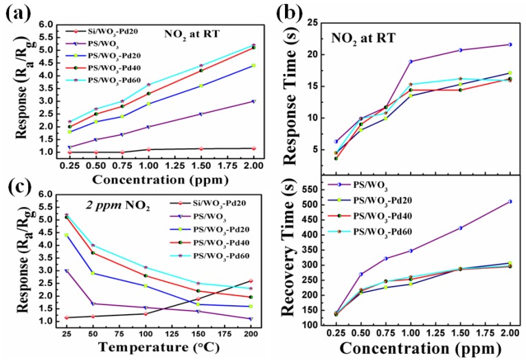
The decoration of noble metal nanoparticles (NPs) on the surface of metal oxide semiconductors to enhance material characteristics and gas-sensing performance has recently attracted increasing attention from researchers worldwide. Here, we have synthesized porous silicon (PS)/WO₃ nanorods (NRs) functionalized with Pd NPs to enhance NO₂ gas-sensing performance. PS was first prepared using electrochemical methods and worked as a substrate. WO₃ NRs were synthesized by thermally oxidizing W film on the PS substrate. Pd NPs were decorated on the surface of WO₃ NRs via in-situ reduction of the Pd complex solution by using Pluronic P123 as the reducing agent. The gas-sensing characteristics were tested at different gas concentrations and different temperatures ranging from room temperature to 200 °C. Results revealed that, compared with bare PS/WO₃ NRs and Si/WO₃ NRs functionalized with Pd NPs, the Pd-decorated PS/WO₃ NRs exhibited higher and quicker responses to NO₂, with a detection concentration as low as 0.25 ppm and a maximum response at room temperature. The gas-sensing mechanism was also investigated and is discussed in detail. The high surface area to volume ratio of PS and the reaction-absorption mechanism can be explained the enhanced sensing performance.
Keywords: Pd nanoparticles; WO3 nanorods; gas sensor; porous silicon; room temperature.
Conflict of interest statement
The authors declare no conflict of interest.
Figures


References
-
- Qin Y., Li X., Wang F., Hu M. Solvothermally synthesized tungsten oxide nanowires/nanorods for NO2 gas sensor applications. J. Alloy. Compd. 2011;509:8401–8406. doi: 10.1016/j.jallcom.2011.05.100. - DOI
-
- Lu G., Xu J., Sun J., Yu Y., Zhang Y., Liu F. UV-enhanced room temperature NO2 sensor using ZnO nanorods modified with SnO2 nanoparticles. Sens. Actuators B. 2012;162:82–88. doi: 10.1016/j.snb.2011.12.039. - DOI
-
- Penza M., Martucci C., Cassano G. NOx gas sensing characteristics of WO3 thin films activated by noble metals (Pd, Pt, Au) layers. Sens. Actuators B. 1998;50:52–59. doi: 10.1016/S0925-4005(98)00156-7. - DOI
-
- Park S. Acetone gas detection using TiO2 nanoparticles functionalized In2O3 nanowires for diagnosis of diabetes. J. Alloy. Compd. 2017;696:655–662. doi: 10.1016/j.jallcom.2016.11.298. - DOI
LinkOut - more resources
Full Text Sources
Other Literature Sources
