. 2018 Mar 21;28(12):1701269.
doi: 10.1002/adfm.201701269. Epub 2017 Jul 19.

A Materials Roadmap to Functional Neural Interface Design

Affiliations

A Materials Roadmap to Functional Neural Interface Design

Steven M Wellman et al. Adv Funct Mater. .

Abstract

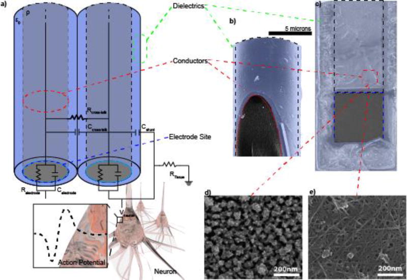
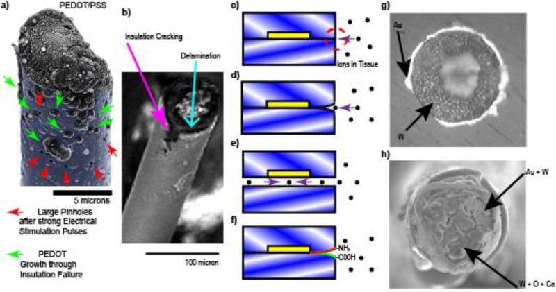
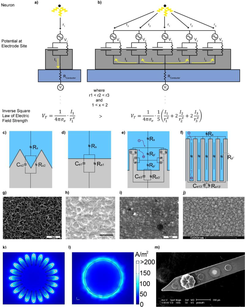
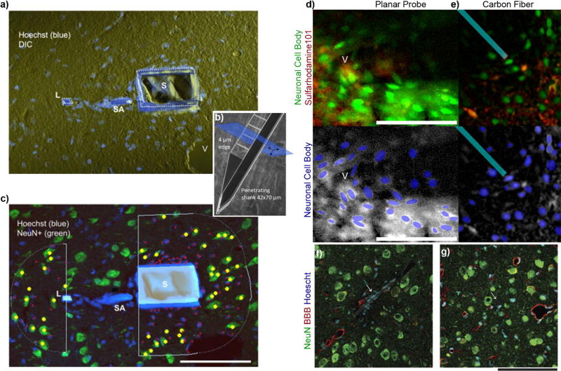
Advancement in neurotechnologies for electrophysiology, neurochemical sensing, neuromodulation, and optogenetics are revolutionizing scientific understanding of the brain while enabling treatments, cures, and preventative measures for a variety of neurological disorders. The grand challenge in neural interface engineering is to seamlessly integrate the interface between neurobiology and engineered technology, to record from and modulate neurons over chronic timescales. However, the biological inflammatory response to implants, neural degeneration, and long-term material stability diminish the quality of interface overtime. Recent advances in functional materials have been aimed at engineering solutions for chronic neural interfaces. Yet, the development and deployment of neural interfaces designed from novel materials have introduced new challenges that have largely avoided being addressed. Many engineering efforts that solely focus on optimizing individual probe design parameters, such as softness or flexibility, downplay critical multi-dimensional interactions between different physical properties of the device that contribute to overall performance and biocompatibility. Moreover, the use of these new materials present substantial new difficulties that must be addressed before regulatory approval for use in human patients will be achievable. In this review, the interdependence of different electrode components are highlighted to demonstrate the current materials-based challenges facing the field of neural interface engineering.

Keywords: Bioelectronics; Electrodes; Microelectromechanical Systems; Photonics; Sensors/Biosensors.


Figures

Figure 1
Figure 1. Basic Electrode Anatomy
a) Randles circuit representation of the electrode, which includes the electrode trace (red dash), insulation (green dash), and electrode site (blue dash: Relectrode and Celectrode) where neural potentials (Vneuron) are recorded from. Note: Post-electrode equipment is not shown. b) Cross-section of a Microthread Electrode[251] showing the carbon fiber core and Parylene insulation. c) Layer-by-Layer (LbL) assembled composite electrodes using Au nanoparticles (d) or carbon nanotubes (e). Reprinted with permission from[569] Copyright 2012, American Chemical Society.
Figure 2
Figure 2. Insulation Failures
a) Strong stimulation currents lead to insulation failure that starts as pin hole defects (Red Arrow) in the insulation (cyan). Complete Insulation failure (green arrow) can be identified over regions of PEDOT/PSS electrochemical deposition through the insulation (cyan). b) Many dielectric polymers such as parylene are susceptible to cracking (magenta arrow) and delamination (cyan arrow). © IOP Publishing. Reproduced with Permission from[210]. All rights Reserved. c) Planar arrays made from crystalline polymers form triple junctions (red dashed circle) when implanted. The two crystalline layers cannot be perfectly aligned due to entropy (blue/white angles). d) Ions and water molecules in the tissue thermodynamically degrade the interface of the two crystalline layers forming a crack. e) Cracks thermodynamically propagate until insulation fails. Note: this is not an issue if the triple junction crack propagation failure rate is slower than the lifetime of the patient. f) Self-healing smart polymers with self-annealing functional groups and re-seal delamination. g) Insulation adhesion layers (eg. Au) are sometimes used to reduce insulation delamination failures. h) In the tissue, the wire (W), exposed adhesion layers (Au), and the tissue environment creates a galvanic cell, accelerating corrosion. Reprinted with permission from[209] Copyright 2011, Elsevier
Figure 3
Figure 3. Electrode site size and material properties influence recording and stimulating performance
A small contact site surface area (a) compared to a larger contact site surface area (b) records larger voltage amplitudes (VT) from a single point source (a neuron) provided by the inverse square law of electric field strength. Note: I2 and I3 are negative. c–f) Charge transfer during electrical stimulation with varying geometric surface areas at the electrode interface. Increasing surface area from (c) to (d) increases the capacitance (Ce2 > Ce1) and halves the resistance (Re1 > Re2). Creating a pore (e) introduces a resistance (Rp’) with a cross-sectional area of A and length l. Increasing pore length from (e) to (f) begins to impact ion movement within the electrode-tissue interface and attenuates electrode performance. g–j) SEM images of electrode site materials: PEDOT/CNT, scale bar 1 µm (g), PEDOT/GO, scale bar 1 µm (h), PEDOT/PSS, scale bar 1 µm (i), and IrOx, scale bar 500 nm (j). Reproduced with permisison from[238],[75], and[570] Copyright, 2016, 2013, and 2010 from IEEE, the Royal Society of Chemistry, and Elsevier, respectively. k,l) Distribution of charge density representing the edge effect for a planar high-surface area electrode (k) and circular electrode (l). Adapted with permission from[183]. Copyright 2009, Frontiers Media SA. m) Recording site electrochemically deposited with polypyrrole (PPy). The octagonal recording site geometry allowed the polymer to grow into eight teardrop segments with an absence of coating from the center. (c–f,m) Reprinted with permisison from[28] Copyright © 2014, Springer Science+Business Media New York
Figure 4
Figure 4. Implant size impacts acute and chronic tissue integration
a) Tissue around the probe’s (b) thin polymer lattice structure showed significant reduction in encapsulating cells and improved neural density (c). (Adapted with permission from[256, 392]). d–e) Two photon imaging of tissue strain in vivo from a Michigan Electrode Array (d) and carbon fiber microthread electrode (e). Neurons are green, while recording sites and astrocytes are red. Cyan outline highlights microthread electrode. Neurons in panel c are much more compressed and oval/elliptical than neurons in panel d, indicating increased mechanical strain from the embedded electrode volume. Reprinted with permission from[34] Copyright 2014, Elsevier. f–g) Chronic histology shows carbon fiber microthreads with an 8-µm diameter reduced tissue reactivity and improved neuron density of microthread (g) compared to silicon electrodes. Reprinted from[128] Copyright 2012, with permission from Nature Publishing Group.
FIGURE 5
FIGURE 5. Probe insertion results in high strain between shanks of multi-shank devices, with more strain generated between densely packed shanks
A finite element simulation of Michigan-style planar silicon probe insertion into a visco-elastic brain phantom is shown. The maximum strain value of each element following insertion is displayed. a) When the probe shanks are spread far apart (500 µm tip-to-tip spacing), there is little overlapping strain between shanks. b–c) As tip-to-tip spacing gets tighter, there is increased tissue strain between shanks (300 and 150 µm). Scale bar = 100 microns.
Figure 6
Figure 6. Mechanical failure from non-homogenous components and geometries
a) A finite element model (FEM) of mechanical strain on a planar silicon array with iridium electrode sites under a 1 micron micromotion in tissue. b) A strain profile along the protruding electrical trace (red dashed line), substrate surface (black solid line), and at the center of the substrate (blue dash dot line) as indicated in (a). c) Strain profile of (a) from the top view. Lowest strain (black) and highest strain (purple) regions are indicated with arrows. (d) SEM of a planar silicon array explanted 189 days post implant in mice V1 cortex. e) 2× zoom in of (d). f) FEM showing an order of magnitude less, evenly distributed strain profiles along simple elegant geometries. Adapted from[35]. Copyright 2015, with permission from Elsevier.
Figure 7
Figure 7. Schematic of different neural probe packaging strategies
Most commercially available technologies are anchored to the skull by cement or bone screws in order to achieve mechanical stability (Top). The platforms and shanks of a device can either be directly attached to the connector (Rigidly anchored) or attached to a wire bundle intermediary (Tethered). Next generation devices could be Unanchored (Bottom). These devices would use telemetry to send neural data to external neural processors. Inset: meningeal fibrosis of the wire bundle of a Utah array that was implanted in a non-human primate for ~4 years (Inset, top). Second-harmonic generation imaging of fibrous tissue around wire bundle shows thick collagenous tissue (~500 µm thick) surrounding wire bundle (Inset, bottom). Non-human primate data is courtesy of the Batista Lab, University of Pittsburgh
Figure 8
Figure 8. Microglial encapsulation of neural probes is attenuated by L1 cell adhesion molecule coating
Both ultrasmall carbon fiber microthread electrodes (left, blue outline) and silicon Michigan microelectrodes (middle, blue outline) are encapsulated by microglial processes (green) after 6 h of implantation in mice. Electrode devices can be “camouflaged” by covalently attaching bioactive molecules to their surfaces, as shown by an L1 cell adhesion molecule coated Michigan electrode (left, blue outline), which is relatively unburdened by microglial encapsulation. Adapted with permission from[8] Copyright 2015, American Chemical Society and from[472] Copyright 2017, Elsevier.
Figure 9
Figure 9. Sample light delivery systems for optogenetic stimulation
a) Optroelectrode design using gallium nitrate (GaN) micro-light emitting diodes (μLEDs) and electrode recording sites stacked together using heterogenous packaging. Reproduced with permission from[318] Copyright 2013, American Association for the Advancement of Science. b) Cross-section along a monolithically fabricated μLED and microelectrode (dash-line on top inset, bottom inset shows the layers along the cross-section). The electrode typically consists of low impedance materials like iridium deposited on layers of SiO2 (green). Gallium nitride (GaN) multi-quantum wells (MQW) are connected to an anode and cathode to form the LED and silicone shank is the base layer. Reproduced with permission from[511] Copyright 2015, Elsevier. c) Organic LED (OLED) layers have also been recently demonstrated in vitro using these dimensions. Potential failure of LED-based illuminating systems is the possibility of failure of the deposited materials and water ingress to leak the voltage to power the LED into the surrounding tissue. This will electrically stimulate the tissue instead of optically. Adapted with permission form[513], Copyright 2016. The American Association for the Advancement of Science. (d–e) Another prototype of optrode where a waveguide is used to deliver light. e) Waveguide cross section showing the transmission, cladding, and silicon substrate layers. Reproduced with permission form[527] Copyright 2015, Nature Publishing Group.
Figure 10
Figure 10. Device considerations and challenges encountered during electrode design in the central nervous system and peripheral nervous system
Axes rank design components from lowest to highest priority for both PNS and CNS devices. Note that device challenges between the two systems are not mutually exclusive. For example, foreign body response is not as disruptive in the PNS (moderate priority) than the CNS (high priority).
Figure 11
Figure 11. Complexity of Functional Neural Interface Engineering
There is a complex network of interdependence between design properties and material constraints, which must be carefully considered when engineering functional neural interface devices. Optimizing a single material property can often negatively impact another material characteristics directly or indirectly through downstream relationships. This can push the overall design outside functional performance constraint windows, ultimately resulting in a non-functional device. Therefore, neural interface engineering requires precise balancing between intrinsic and extrinsic material properties, and their impact on overall performance. Bolded words represent tunable design parameters, and italics denote influencing factors or constraints. Functional performance characteristics are listed in the center, where the biological, electrical and mechanical domains overlap. Blue and red arrows represent positive or negative correlations between terms. Abbreviations include BBB (blood brain barrier), PC (pseudocapacitive), µ/n (micro/nano surface), ESA:GSA (electrochemical to geometric surface area ratio), VD (volumetric density of tissue recording). See Table 1 for simplified form.

References

    1. Huber D, Gutnisky DA, Peron S, O'Connor DH, Wiegert JS, Tian L, Oertner TG, Looger LL, Svoboda K. Nature. 2012;484:473. - PMC - PubMed
    1. Collinger JL, Kryger MA, Barbara R, Betler T, Bowsher K, Brown EH, Clanton ST, Degenhart AD, Foldes ST, Gaunt RA, Gyulai FE, Harchick EA, Harrington D, Helder JB, Hemmes T, Johannes MS, Katyal KD, Ling GS, McMorland AJ, Palko K, Para MP, Scheuermann J, Schwartz AB, Skidmore ER, Solzbacher F, Srikameswaran AV, Swanson DP, Swetz S, Tyler-Kabara EC, Velliste M, Wang W, Weber DJ, Wodlinger B, Boninger ML. Clin Transl Sci. 2014;7:52. - PMC - PubMed
    1. Hochberg LR, Serruya MD, Friehs GM, Mukand JA, Saleh M, Caplan AH, Branner A, Chen D, Penn RD, Donoghue JP. Nature. 2006;442:164. - PubMed
    1. Collinger JL, Wodlinger B, Downey JE, Wang W, Tyler-Kabara EC, Weber DJ, McMorland AJ, Velliste M, Boninger ML, Schwartz AB. Lancet. 2013;381:557. - PMC - PubMed
    1. Barrese JC, Rao N, Paroo K, Triebwasser C, Vargas-Irwin C, Franquemont L, Donoghue JP. Journal of Neural Engineering. 2013;10:066014. - PMC - PubMed