. 2018 Jun 6;18(6):1857.
doi: 10.3390/s18061857.

One-Step Laser Patterned Highly Uniform Reduced Graphene Oxide Thin Films for Circuit-Enabled Tattoo and Flexible Humidity Sensor Application

Affiliations

One-Step Laser Patterned Highly Uniform Reduced Graphene Oxide Thin Films for Circuit-Enabled Tattoo and Flexible Humidity Sensor Application

Rowoon Park et al. Sensors (Basel). .

Abstract

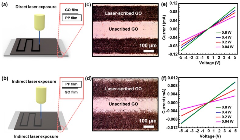
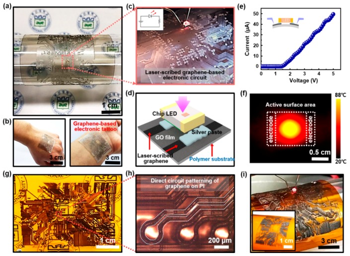
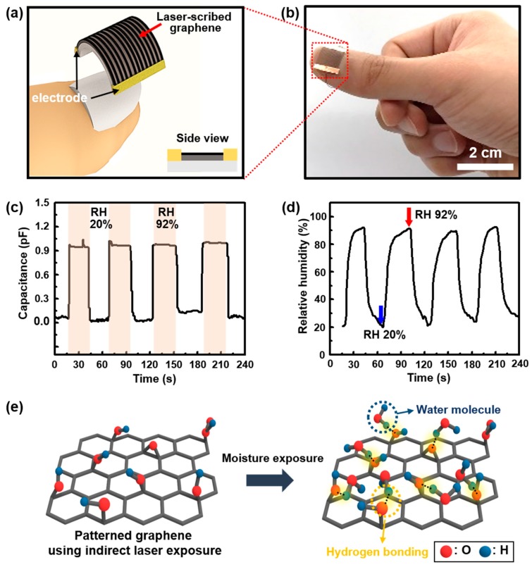
The conversion of graphene oxide (GO) into reduced graphene oxide (rGO) is imperative for the electronic device applications of graphene-based materials. Efficient and cost-effective fabrication of highly uniform GO films and the successive reduction into rGO on a large area is still a cumbersome task through conventional protocols. Improved film casting of GO sheets on a polymeric substrate with quick and green reduction processes has a potential that may establish a path to the practical flexible electronics. Herein, we report a facile deposition process of GO on flexible polymer substrates to create highly uniform thin films over a large area by a flow-enabled self-assembly approach. The self-assembly of GO sheets was successfully performed by dragging the trapped solution of GO in confined geometry, which consisted of an upper stationary blade and a lower moving substrate on a motorized translational stage. The prepared GO thin films could be selectively reduced and facilitated from the simple laser direct writing process for programmable circuit printing with the desired configuration and less sample damage due to the non-contact mode operation without the use of photolithography, toxic chemistry, or high-temperature reduction methods. Furthermore, two different modes of the laser operating system for the reduction of GO films turned out to be valuable for the construction of novel graphene-based high-throughput electrical circuit boards compatible with integrating electronic module chips and flexible humidity sensors.

Keywords: circuit; graphene oxide; humidity sensor; laser-exposure; self-assembly.


Conflict of interest statement

The authors declare no conflicts of interest.

Figures

Figure 1
Figure 1
Fabrication process of the uniformly deposited GO thin film on a polymer substrate via flow-enabled self-assembly. (a) Schematic illustration of the self-assembly of GO sheets by dragging the trapped GO colloidal solution in restricted geometry consisted of an upper tilted stationary blade and a lower moving substrate on a motorized translational stage. (b) Schematic side-view illustrates the evaporative shear flow induced deposition of GO sheets at the end of the meniscus on a flat substrate. (c) Scanning Electron Microscope (SEM) image (left) and Atom Force Microscope (AFM) image (right) of the highly uniform GO thin film formed on a substrate. (d) Schematic steps for the surface modification of polymer substrate (i.e., PP) using mild oxygen plasma and the successive self-assembled monolayer treatment of APTES.
Figure 2
Figure 2
(a) Schematic illustration of UV pulse laser system for the reduction of GO. (b) Digital image of university logo with sharp contrast (inset) engraved by laser direct writing (LDW) on GO coated PP substrate, showing optical properties with see-through type transparency.
Figure 3
Figure 3
Laser-scribed patterning and reduction of GO thin films formed on PP substrate to fabricate rGO-GO-rGO stripes with a controlled mode of operation. (a) Direct laser exposure on GO-PP substrate. (b) Indirect laser exposure on GO film through PP barrier. The inset drawings in figure (a,b) illustrates the surface position of GO film and PP substrate against the laser exposure. (c,d) Optical micrographs showing the patterned rGO-GO-rGO stripes operated by direct and indirect laser exposure (dark lines: laser-scribed rGO, bright line: unscribed pristine GO). (e,f) Typical I-V characteristics of the samples scribed by direct and indirect laser operations.
Figure 4
Figure 4
(a) Digital image of laser-scribed rGO patterned arrays connected to copper electrodes on a flexible PP substrate. (b) Macroscopic SEM image of the laser-scribed GO film (bright lines: laser-scribed rGO, black lines: unscribed pristine GO). (c) SEM image of the close-up surface area in (b) with swollen microstructural hierarchies. (d) Raman spectra of laser-scribed GO (black) and GO (red) indicate the reduction of GO film in the range of 1300−3000 cm−1. (e) Raman mapping image of GO-rGO-GO region. (f) AFM image at the boundary between the laser-scribed rGO and pristine GO film marked by dotted white line; green line shows relative height profile, ~500 nm.
Figure 5
Figure 5
Graphene-based flexible electronic circuit boards produced via programmable direct laser-scribing. (a) Digital image of the representative flexible circuit board filled with the patterned rGO circuital lines, wrapped around a curved glass-tube surface. (b) Graphene-based electronic-tattoo attached on a wrist and back of a hand. (c) Light-up a surface-mounted LED integrated on an rGO-based circuit board in (a). (d) Schematic illustration of a chip LED bonded onto the isolated two terminal pads using silver-based solder paste. (e) Typical I-V characteristics of a chip LED integrated on the circuit board at bending state. (f) Thermographic image from a sticky plastic electronic tattoo (i.e., rGO-based microheater); thermal distribution ranged between 20 to 80 °C. (g) Digital image of the flexible circuit board prepared by direct laser-scribing of Kapton film. (h) Magnified OM image of a discretely patterned surface on the Kapton film; the white dotted lines indicate the laser-scribed conductive circuital lines. (i) Light-up a surface-mounted LED integrated on the two-terminal rGO circuit pads embedded on Kapton film.
Figure 6
Figure 6
Schematic view (a) and digital image (b) of the laser-scribed rGO-based flexible humidity sensor attached on a nail (e.g., press-on nail wearable sensor), consisting of an indirect laser-scribed rGO film on flexible PP substrate integrated with a copper electrode. (c) The real-time signal responses as measured cyclic capacitance changes from the LDW GO-based humidity sensor, exposed to RH in the range of 20% to 92% at 30 s intervals. (d) The monitored RH changes collected from the real-time data logger correspond to the graph in (c). (e) Schematic drawing of absorption process of water molecules by hydrogen bonding on the partially reduced GO surface after moisture exposure.

References

    1. Novoselov K.S., Geim A.K., Morozov S.V., Jiang D., Zhang Y., Dubonos S.V., Grigorieva I.V., Firsov A.A. Electric field effect in atomically thin carbon films. Science. 2004;306:666–669. doi: 10.1126/science.1102896. - DOI - PubMed
    1. Mak K.F., Shan J., Heinz T.F. Electronic structure of few-layer graphene: experimental demonstration of strong dependence on stacking sequence. Phys. Rev. Lett. 2010;104:176404. doi: 10.1103/PhysRevLett.104.176404. - DOI - PubMed
    1. Chen J., Duan M., Chen G. Continuous mechanical exfoliation of graphene sheets via three-roll mill. J. Mater. Chem. 2012;22:19625–19628. doi: 10.1039/c2jm33740a. - DOI
    1. Somani P.R., Somani S.P., Umeno M. Planer nano-graphenes from camphor by CVD. Chem. Phys. Lett. 2006;430:56–59. doi: 10.1016/j.cplett.2006.06.081. - DOI
    1. Bo Z., Yang Y., Chen J., Yu K., Yan J., Cen K. Plasma-enhanced chemical vapor deposition synthesis of vertically oriented graphene nanosheets. Nanoscale. 2013;5:5180–5204. doi: 10.1039/c3nr33449j. - DOI - PubMed