Microfluidic devices for small-angle neutron scattering
- PMID: 29896054
- PMCID: PMC5988002
- DOI: 10.1107/S1600576718007264
Microfluidic devices for small-angle neutron scattering
Abstract
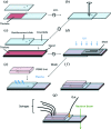
A comparative examination is presented of materials and approaches for the fabrication of microfluidic devices for small-angle neutron scattering (SANS). Representative inorganic glasses, metals, and polymer materials and devices are evaluated under typical SANS configurations. Performance criteria include neutron absorption, scattering background and activation, as well as spatial resolution, chemical compatibility and pressure resistance, and also cost, durability and manufacturability. Closed-face polymer photolithography between boron-free glass (or quartz) plates emerges as an attractive approach for rapidly prototyped microfluidic SANS devices, with transmissions up to ∼98% and background similar to a standard liquid cell (I ≃ 10-3 cm-1). For applications requiring higher durability and/or chemical, thermal and pressure resistance, sintered or etched boron-free glass and silicon devices offer superior performance, at the expense of various fabrication requirements, and are increasingly available commercially.
Keywords: closed-face polymer photolithography; lab-on-a-chip; microfluidic devices; small-angle neutron scattering.
Figures


Similar articles
-
Microfluidic-SANS: flow processing of complex fluids.Sci Rep. 2015 Jan 12;5:7727. doi: 10.1038/srep07727. Sci Rep. 2015. PMID: 25578326 Free PMC article.
-
A more informative approach for characterization of polymer monolithic phases: small angle neutron scattering/ultrasmall angle neutron scattering.Anal Chem. 2011 Dec 15;83(24):9201-5. doi: 10.1021/ac202238r. Epub 2011 Nov 15. Anal Chem. 2011. PMID: 22066706
-
A novel small-angle neutron scattering detector geometry.J Appl Crystallogr. 2013 Aug 1;46(Pt 4):1031-1037. doi: 10.1107/S0021889813011862. Epub 2013 Jul 4. J Appl Crystallogr. 2013. PMID: 24046504 Free PMC article.
-
Small Angle Neutron Scattering in Drug Discovery Research: A Novel Tool for Advanced Study of Structures of Biological Macromolecules.Curr Drug Discov Technol. 2023;20(5):e150523216942. doi: 10.2174/1570163820666230515162614. Curr Drug Discov Technol. 2023. PMID: 37190797 Review.
-
Biological small-angle neutron scattering: recent results and development.Acta Crystallogr D Struct Biol. 2018 Aug 1;74(Pt 8):715-726. doi: 10.1107/S2059798318005016. Epub 2018 Jul 17. Acta Crystallogr D Struct Biol. 2018. PMID: 30082507 Review.
Cited by
-
A novel experimental approach for nanostructure analysis: simultaneous small-angle X-ray and neutron scattering.J Appl Crystallogr. 2020 May 13;53(Pt 3):722-733. doi: 10.1107/S1600576720005208. eCollection 2020 Jun 1. J Appl Crystallogr. 2020. PMID: 32684887 Free PMC article.
-
Microfluidic Nanomaterial Synthesis and In Situ SAXS, WAXS, or SANS Characterization: Manipulation of Size Characteristics and Online Elucidation of Dynamic Structural Transitions.Molecules. 2022 Jul 19;27(14):4602. doi: 10.3390/molecules27144602. Molecules. 2022. PMID: 35889473 Free PMC article. Review.
-
Free-film small-angle neutron scattering: a novel container-free in situ sample environment with minimized H/D exchange.J Appl Crystallogr. 2019 Feb 26;52(Pt 2):284-288. doi: 10.1107/S1600576719000906. eCollection 2019 Apr 1. J Appl Crystallogr. 2019. PMID: 30996715 Free PMC article.
-
Construction of Bone Hypoxic Microenvironment Based on Bone-on-a-Chip Platforms.Int J Mol Sci. 2023 Apr 10;24(8):6999. doi: 10.3390/ijms24086999. Int J Mol Sci. 2023. PMID: 37108162 Free PMC article. Review.
-
In situ small-angle X-ray scattering measurement at the Very Small Angle Neutron Scattering Instrument at the China Spallation Neutron Source.J Appl Crystallogr. 2025 Feb 28;58(Pt 2):573-580. doi: 10.1107/S1600576725001232. eCollection 2025 Apr 1. J Appl Crystallogr. 2025. PMID: 40170974 Free PMC article.
References
-
- Adamo, M., Poulos, A. S., Lopez, C. G., Martel, A., Porcar, L. & Cabral, J. T. (2018). Soft Matter, 14, 1759–1770. - PubMed
-
- Adamo, M., Poulos, A., Miller, R. M., Lopez, C. G., Martel, A., Porcar, L. & Cabral, J. T. (2017). Lab Chip, 17, 1559–1569. - PubMed
-
- Adams, D. P., Vasile, M. J., Benavides, G. & Campbell, A. N. (2001). Precision Eng. 25, 107–113.
-
- Bailey, I. (2003). Z. Kristallogr. Cryst. Mater. 218, 84–95.
Publication types
LinkOut - more resources
Full Text Sources
Other Literature Sources
Miscellaneous
