. 2018 Jul 11;18(7):4241-4246.
doi: 10.1021/acs.nanolett.8b01223. Epub 2018 Jun 27.

Moiré-Modulated Conductance of Hexagonal Boron Nitride Tunnel Barriers

Affiliations

Moiré-Modulated Conductance of Hexagonal Boron Nitride Tunnel Barriers

Alex Summerfield et al. Nano Lett. .

Abstract

Monolayer hexagonal boron nitride (hBN) tunnel barriers investigated using conductive atomic force microscopy reveal moiré patterns in the spatial maps of their tunnel conductance consistent with the formation of a moiré superlattice between the hBN and an underlying highly ordered pyrolytic graphite (HOPG) substrate. This variation is attributed to a periodc modulation of the local density of states and occurs for both exfoliated hBN barriers and epitaxially grown layers. The epitaxial barriers also exhibit enhanced conductance at localized subnanometer regions which are attributed to exposure of the substrate to a nitrogen plasma source during the high temperature growth process. Our results show clearly a spatial periodicity of tunnel current due to the formation of a moiré superlattice and we argue that this can provide a mechanism for elastic scattering of charge carriers for similar interfaces embedded in graphene/hBN resonant tunnel diodes.

Keywords: Boron nitride; epitaxy; growth; heterostructure; moiré; superlattice; tunneling.


Conflict of interest statement

The authors declare no competing financial interest.

Figures
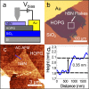
Figure 1
Figure 1
(a) Schematic of exfoliated hBN/HOPG tunnel barrier device. (b) Bright-field optical image of the device. The white box indicates the approximate position of the exfoliated hBN flakes. Dark-field optical imaging of this region is given in the Supporting Information, see Figure S1. (c) AC-mode AFM image of part of the region indicated by the white box in image (b), showing a monolayer hBN flake. (d) Line profile along the region indicated by the blue line in (c) demonstrating the monolayer thickness of the exfoliated hBN flake.
Figure 2
Figure 2
cAFM images of the exfoliated hBN/HOPG device shown in Figure 1. (a) Height-channel image of the surface topography of hBN. (b) Current map of the same area as in image (a), exhibiting an 11.7 nm moiré pattern due to rotational misalignment between the hBN and HOPG lattices (cAFM tip bias: +10 mV). (c) (top) Height profile along the line indicated in (a). (bottom) Conductance profile along the line indicated in (b) showing a spatial variation in tunnel current across the hBN surface (bottom). (d) Contact mode lattice image showing the hBN lattice and expected hBN periodicity.
Figure 3
Figure 3
(a) Schematic of PA-MBE hBN/HOPG device and the experimental setup for cAFM imaging. (b) Contact mode AFM image of MBE hBN on HOPG; the arrow indicates a region of HOPG not covered by PA-hBN growth. (c) Contact mode AFM images of multiple hBN domains around a small region of HOPG not covered by hBN growth (dark indicated area). (d) Height profile along the red line in (c) indicating the monolayer hBN thickness.
Figure 4
Figure 4
Topographic and cAFM images of PA-MBE grown hBN on HOPG; the label in each image indicates the imaging mode (top label) and/or the surface being imaged (bottom left label). (a) Contact-mode AFM image showing PA-MBE hBN domains with an exposed area of HOPG indicted by the labels. The boxes show the positions of the high-resolution scans of the hBN domains for images (c,e). (inset) Line profiles along the regions indicated by the blue and red lines in (a,b) respectively at an interface between PA-MBE hBN and exposed HOPG. (b) Current channel image of the top half of (a). The labeled boxes correspond to the same regions labeled in (a), showing where high resolutions scans were taken. (c) Tunnel current map of the region indicated by the topmost white box in image (b) showing a moiré pattern with a period of 13.5 nm. (d) Line profile across the white line in image (c) showing the variation in tunnel current. (e) Tunnel current channel image of non-aligned PA-hBN exhibiting no moiré pattern in the current signal. (f) Current map of an exposed HOPG region with no hBN overgrowth. (g) Contact mode AFM image showing the hBN lattice. (h) Tunnel current channel of (b) showing localized hot-spots of increased conductance. (i) Height profile (top) and tunnel current profile (bottom) along the blue and red lines marked in (g,h) respectively. All cAFM images were taken with a tip bias of +100 mV with the exception of (h) which was acquired using a tip bias of +10 mV.
Figure 5
Figure 5
Constant current STM images of hBN grown on HOPG using PA-MBE. (a) STM image showing multiple domains of hBN grown on HOPG. The white boxes indicate the regions shown in images (b,d,i), respectively. (b) Moiré patterns visible on either side of the boundary between two hBN domains, indicated by the white box in (a). The moiré periods on the left and right domains are 16 and 14 nm, respectively. (c) STM image of a monolayer hBN domain on HOPG without moiré patterns showing small regions of increased brightness (i.e., higher STM topography). The profiles indicated by the colored lines are shown in (j). (d) STM image of a bilayer (BL) hBN domain surrounded by monolayer (ML) hBN as indicated by the box in (a). (e) Moiré patterns visible on ML hBN region in (d). (f) Zoom of (e) showing lattice-level contrast of ML hBN domain. (g) STM image of moiré patterns visible on BL hBN domain shown in (d). (h) Zoom of (g) showing lattice-level contrast of BL hBN. (i) STM image showing border between ML and BL hBN as indicated by the white box in (a). In both regions, moiré patterns are visible and have a periodicity of 2.4 ± 0.1 nm for both the ML and BL regions, respectively. (j) Constant current profiles along the lines indicated in (c) showing small regions with increased tunnel conductance.

References

    1. Dean C. R.; Young A. F.; Meric I.; Lee C.; Wang L.; Sorgenfrei S.; Watanabe K.; Taniguchi T.; Kim P.; Shepard K. L.; Hone J. Nat. Nanotechnol. 2010, 5, 722–726. 10.1038/nnano.2010.172. - DOI - PubMed
    1. Novoselov K. S.; Geim A. K.; Morozov S. V.; Jiang D.; Zhang Y.; Dubonos S. V.; Grigorieva I. V.; Firsov A. A. Science 2004, 306, 666–669. 10.1126/science.1102896. - DOI - PubMed
    1. Yankowitz M.; Xue J.; Cormode D.; Sanchez-Yamagishi J. D.; Watanabe K.; Taniguchi T.; Jarillo-Herrero P.; Jacquod P.; LeRoy B. J. Nat. Phys. 2012, 8, 382–386. 10.1038/nphys2272. - DOI
    1. Britnell L.; Gorbachev R. V.; Jalil R.; Belle B. D.; Schedin F.; Mishchenko A.; Georgiou T.; Katsnelson M. I.; Eaves L.; Morozov S. V.; Peres N. M. R.; Leist J.; Geim A. K.; Novoselov K. S.; Ponomarenko L. A. Science 2012, 335, 947–950. 10.1126/science.1218461. - DOI - PubMed
    1. Dean C. R.; Wang L.; Maher P.; Forsythe C.; Ghahari F.; Gao Y.; Katoch J.; Ishigami M.; Moon P.; Koshino M.; Taniguchi T.; Watanabe K.; Shepard K. L.; Hone J.; Kim P. Nature 2013, 497, 598–602. 10.1038/nature12186. - DOI - PubMed

Publication types

LinkOut - more resources