Review
. 2018 Jun 26;8(7):463.
doi: 10.3390/nano8070463.

Properties, Preparation and Applications of Low Dimensional Transition Metal Dichalcogenides

Affiliations
Review

Properties, Preparation and Applications of Low Dimensional Transition Metal Dichalcogenides

Lei Yang et al. Nanomaterials (Basel). .

Abstract

Low-dimensional layered transition metal dichalcogenides (TMDs) have recently emerged as an important fundamental research material because of their unique structural, physical and chemical properties. These novel properties make these TMDs a suitable candidate in numerous potential applications. In this review, we briefly summarize the properties of low-dimensional TMDs, and then focus on the various methods used in their preparation. The use of TMDs in electronic devices, optoelectronic devices, electrocatalysts, biosystems, and hydrogen storage is also explored. The cutting-edge future development probabilities of these materials and numerous research challenges are also outlined in this review.

Keywords: chemical vapor deposition; crystal structure; electronic structure; low dimensional transition metal dichalcogenides; preparation methods.


Conflict of interest statement

The authors declare no conflicts of interest.

Figures

Figure 1
Figure 1
Structure of low-dimensional TMDs. (a) Three-dimensional schematic representation of a typical MX2 structure. The yellow balls and grey balls refer to chalcogen atoms and transition metal atoms, respectively [70]. (b) The layer structure (top) and rectangular unit cell (down) of 2H, 1T and 1T’ phases. The 2H phase refer to trigonal prismatic structure, 1T and 1T’are called octahedral and distorted octahedral, respectively [71]. (c) Schematic structure of 2H, 3R and 1T phase of MX2. The interlayer spacing is ~6.5 Å and the stacking index c indicates the number of layers in each stacking order [70]. (d) Schematic illustration of the gliding of S plane (top) and Mo plane (bottom), which result in phase transition. The S plane glide results in a 2H → 1T phase transition, and Mo plane glide results in a 2H → 2H’ transition, where the 2H’ phase is a 60° rotational phase of 2H [73]. (e) HRSTEM image of monolayer WSe2 with defect-free atomic lattices. The W and Se atoms form the hexagonal ring with different brightness as denoted by the color cartoon spheres [43]. (f,g) Schematic illustration and HRSTEM image of MoS2 nanobelts. The vertical atomic layers form the nanobelt structure, and these layer edges form the top surface of the nanobelt [80]. (h) Side and top views of the structures of 8-zigzag MoS2 nanoribbon (top) and 15-armchair MoS2 nanoribbon (down). The Wz (Wa) and dz (da) correspond to the ribbon width and 1-D unit cell distance, respectively [27]. (i) Armchair (8, 8) MoS2 nanotube (left) and zigzag (14, 0) MoS2 nanotube (right). The dark and light atoms are Mo and S, respectively [81]. Reproduced with permission from [27]. Copyright American Chemical Society, 2008. Reproduced with permission from [43]. Copyright The Royal Society of Chemistry, 2015. Reproduced with permission from [70]. Copyright Macmillan Publishers Limited, 2012. Reproduced with permission from [71,73]. Copyright Macmillan Publishers Limited, 2014. Reproduced with permission from [80]. Copyright American Chemical Society, 2015. Reproduced with permission from [81]. Copyright The American Physical Society, 2000.
Figure 2
Figure 2
Band structure and optical properties of low-dimensional TMDs. (a) Calculated band structures of bulk MoS2, quadrilayer MoS2, bilayer MoS2 and monolayer MoS2. Bulk MoS2, quadrilayer MoS2, bilayer MoS2 are all indirect band gap materials. When the thickness is reduced, the indirect band gap becomes larger. It becomes direct band gap when the thickness reaches the 2D limit [95]. (b) PL spectra of MoS2 with different thickness (1–6 layers). Peak I corresponds to the indirect band gap transition, while peaks A and B refer to the direct band gap transition [21]. (c) Schematic view of the atomic displacements of the four Raman-active modes [39]. (d) Raman spectra of MoS2 with different thickness. With increasing the layer from 1 to 6, the E2g1 shows red shifts, and A1g shows blue shifts [96]. (e) The layer dependent of the E2g1 and A1g Raman modes (left vertical axis) and the difference of E2g1 and A1g (right vertical axis) as a function of layer thickness [96]. (f) Raman spectra of monolayer and bilayer WSe2. For bilayer WSe2, there was an obvious peak at 307 cm−1 which was absent in monolayer one [97]. (g) PL spectra of the nanobelt, an exfoliated multilayer, and a CVD-grown monolayer. Compared with exfoliated multilayer, the indirect band gap transition peak nearly disappeared [80]. (h,i) Scheme of the structure and electronic band picture for the nanobelt. The induced excitons first diffuse to the metallic surface and then nonradiatively decay [80]. (j) The relationship between the MoS2 QDs size and bandgap. With reducing the QDs size, reduced band gap was obtained [29]. Reproduced with permission from [21]. Copyright The American Physical Society, 2010. Reproduced with permission from [29]. Copyright AIP Publishing LLC, 2015. Reproduced with permission from [39]. Copyright Macmillan Publishers Limited, 2014. Reproduced with permission from [80]. Copyright American Chemical Society, 2015. Reproduced with permission from [95,96]. Copyright American Chemical Society, 2010. Reproduced with permission from [97]. Copyright American Chemical Society, 2013.
Figure 3
Figure 3
Band gap engineering of low-dimensional TMDs. (a) Schematic illustration of the bending apparatus used to exert strain on MoS2. By controllably bending the polycarbonate beam of the four-point bending apparatus, a uniaxial strain was exerted on monolayer and bilayer MoS2 [110]. (b) Evolution of the Raman spectra with strain ranged from 0 to 1.6%. With increased strain, the symmetry of the crystal broke, which made the degenerate E’ peak split into two sub-peaks [110]. (c) Schematic depiction of the micro-Raman-PL experimental configuration. The surface of the monolayer MoS2 is covered by different solvents during experiments [113]. (d) PL spectra of monolayer MoS2 with different solvent surroundings. The emission peaks were tuned in the range of 1.78–1.90 eV. Red shifts of the monolayer MoS2 PL peaks were observed when the surroundings changed from air to non-halogenated solvents (water, ethanol, dimethyl sulfoxide, propylamine). Blue shifts were observed when the surroundings changed from air to halogenated solvents (trifluoroacetic acid, methylene chloride, chloroform, carbon tetrachloride, butyl bromide, propyl bromide) [113]. (e) UV-visible absorption of functionalized MoS2 QDs. The absorption edges of MoS2 QDs in DI water (H2O-QDs), in DMF and in ethanol were located at ~310 nm, ~260 nm, and ~335 nm, respectively [40]. Reproduced with permission from [40]. Copyright Elsevier Inc., 2017. Reproduced with permission from [110]. Copyright American Chemical Society, 2013. Reproduced with permission from [113]. Copyright Wiley-VCH Verlag GmbH & Co. KGaA, 2013.
Figure 4
Figure 4
Mechanical, ferromagnetic and superconductivity properties of 2D TMDs. (a) Schematic illustration for the stiffness measurements of monolayer MoS2. During measurements, the AFM tip was placed above the center of the suspend area and slowly lowered while monitoring the deflection [117]. (b) Diagrammatic representation of the phase incorporation strategy to achieve ferromagnetism of 2H-MoS2 nanosheets. By incorporating the 1T-MoS2 phase into the 2H-MoS2 matrix, ferromagnetism was induced [118]. (c) Temperature dependence of the square resistance of ionic-gated WS2 FET at VG = 3.7 V. The resistance decrease was observed with an onset at ~4 K, and the resistance reached zero at Tc ~ 0.5 K. The inset shows the magnetic field dependence of the square resistance at T = 0.25 K, which indicated that the WS2 reached the normal state value with magnetic field B ~ 0.14 T [119]. Reproduced with permission from [117]. Copyright American Chemical Society, 2011. Reproduced with permission from [118,119]. Copyright American Chemical Society, 2015.
Figure 5
Figure 5
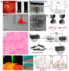
Top-down methods for the preparation of low-dimensional TMDs. (a) AFM image of as-exfoliated NbSe2. The scale bar is 1 μm. The different brightness corresponded to different thickness [30]. (b) Photographs of the dispersions of MoS2 and WS2 in NMP [32]. (c) Photographs of WS2 dispersions in various ethanol/water mixtures, which were stored for a week. The dispersion of WS2 reached its maximum concentration in 35 vol.% ethanol/water [33]. (d) The calculated Ra values (solid line) and the absorbance (dots) of the WS2 in various ethanol/water mixtures [33]. (e) Low-magnification TEM image of the MoS2 QDs. The size distribution of the QDs was shown in the inset, which indicated that the size was in the range of 2–9 nm [29]. (f) High-resolution TEM images of a typical MoS2 QDs. The clear lattice fringe indicated its highly crystalline structure [29]. (g) The illustration of shear and compression effects during the low-energy ball milling process, and the scission and vibration effects during the sonication process. The shear force induced exfoliation and the compression force induced exfoliation (top). Sonication induced scission and vibration induced exfoliation (down) [134]. (h) Optical image of the exfoliated monolayer TaS2 on SiO2/Si substrate. The size ranged from several tens of micrometers to more than 100 μm [135]. (i) Schematic drawing of the electrochemical lithiation process for the fabrication of 2D nanosheets from bulk material [36]. (j) Left: schematic illustration of the laser induced thinning method to prepare monolayer MoS2. Right: optical image of a multilayer MoS2 flake before and after scanned by a laser. The regions with different colors corresponded to different number of layers. After the laser-thinning process, the optical contrast of the rectangle region was uniform, consistent with that of a single MoS2 monolayer [37]. (k,l) Raman and PL spectra of monolayer MoS2 after Ar+ plasma irradiation with different time. On increasing the irradiation from 10 to 85 s, the Raman peaks became weak and broadened, and the PL intensities became much weaker. After 115 s irradiation, the Raman and PL peaks disappeared [38]. Reproduced with permission from [29]. Copyright AIP Publishing LLC, 2015. Reproduced with permission from [30]. Copyright Proceedings of the National Academy of Sciences of the United States of America, 2005. Reproduced with permission from [32]. Copyright American Association for the Advancement of Science, 2011. Reproduced with permission from [33,36]. Copyright Wiley-VCH Verlag GmbH & Co. KGaA, Weinheim, 2011. Reproduced with permission from [37]. Copyright American Chemical Society, 2012. Reproduced with permission from [38]. Copyright American Chemical Society, 2013. Reproduced with permission from [134]. Copyright The Royal Society of Chemistry, 2012. Reproduced with permission from [135]. Copyright American Chemical Society, 2017.
Figure 6
Figure 6
Bottom-up approaches (solid-phase reaction method, hydrothermal method and CVD method) for the preparation of 2D TMDs. (a) SEM image of MoS2 flakes synthesized by solid-phase reaction method. The lateral size of MoS2 flakes could be up to 10 μm, and the thickness was about a few hundred nanometers [143]. (b) SEM image of MoS2 nanosheets synthesized by the hydrothermal method. The 2D MoS2 nanosheets were rolled up and formed a nanoflower morphology [39]. (c) Schematic illustration of the setup for the synthesis of monolayer MoS2. The substrates were placed face-down above the ceramic boat, which was filled with MoO3. Another ceramic boat filled with S powder was located in the upstream of MoO3 [41]. (d) Optical image of monolayer MoS2. The MoS2 showed a uniform morphology with centimeter sizes [42]. (e,f) Optical images of monolayer WSe2 synthesized at different growth temperatures by CVD method. The monolayer WSe2 exhibited the uniform morphologies with several tens microns in size [43]. (g) Schematic depiction of the growth setup for the synthesis of monolayer WS2(1−x)Se2x alloys. The growth was conducted in a two-temperature zone tube furnace, where S and Se powders were placed in the upstream zone, and the WO3 was placed in the downstream zone [108].Reproduced with permission from [39]. Copyright Macmillan Publishers Limited, 2014. Reproduced with permission from [41]. Copyright Wiley-VCH Verlag GmbH & Co. KGaA, Weinheim, 2012. Reproduced with permission from [42]. Copyright American Chemical Society, 2013. Reproduced with permission from [43]. Copyright The Royal Society of Chemistry, 2015. Reproduced with permission from [108]. Copyright Wiley-VCH Verlag GmbH & Co. KGaA, Weinheim, 2015. Reproduced with permission from [143]. Copyright Elsevier B.V., 2017.
Figure 7
Figure 7
CVD synthesis of 1D TMDs. (a,b) SEM images of WO3 nanowires and WS2(1−x)Se2x nanotubes, respectively. The entire surfaces of the CFs were covered vertically and uniformly with high-density WO3 nanowires and WS2(1−x)Se2x nanotubes. The WO3 nanowires showed the length of ∼5 μm and the diameter of ∼100 nm [45]. (c) HRTEM image of WS2(1−x)Se2x nanotubes. The spacing of WS2(1−x)Se2x nanotubes between lattice fringes was 0.6411 nm [45]. (d) Optical image of MoS2 nanobelts. The area coverage was around 5%, and the length was 10~20 μm [80]. (e) Schematic illustration of the growth of MoS2 narrow ribbons. Firstly, the liquid phase Na–Mo–O in small droplets was formed. Then the Na–Mo–O droplet dissolved sulfur. At last, the ribbons grew horizontally and the droplet crawled laterally [50]. (f) Optical image of MoS2 ribbons grown on a NaCl crystal. The ribbons showed the widths of a few tens of nanometers to a few micrometers and lengths ranged from a few to tens of micrometers [50]. Reproduced with permission from [45]. Copyright American Chemical Society, 2014. Reproduced with permission from [50]. Copyright Macmillan Publishers Limited, 2018. Reproduced with permission from [80]. Copyright American Chemical Society, 2015.
Figure 8
Figure 8
Bottom-up approaches (annealing of the (NH4)2MoS4 precursor, chemical vapor transport method and physical vapor deposition method) for the preparation of low-dimensional TMDs. (a) Schematic depiction of the two-step thermolysis process for the synthesis of MoS2 thin layers. The insulating substrate was immersed into the (NH4)2MoS4 solution followed by the two-step annealing process [51]. (b,c) Photographs and schematic illustration of coating of (NH4)2MoS4 on Ni foils and roll-to-roll thermal decomposition for layer-controlled MoS2 on Ni foils [157]. (d) SEM (top) and TEM (down) images of MoS2 nanotubes. The MoS2 nanotube had a typical length of several hundreds of nanometers and a uniform diameter about 50 nm [158]. (e) Typical TEM image of MoS2 nanoribbon. At the edge of the nanoribbon, it showed the wrapping of the layers [54]. (f) Cross-section TEM image of MoS2 nanotubes. The nanotubes had minor and major radii of 5 nm and 20 nm, respectively [54]. (g) Schematic illustration of three-zone furnace for the physical vapor deposition growth of monolayer MoS2(1−x)Se2x. MoSe2 and MoS2 powders were put in the first and second upstream zones, respectively, and the substrate was put in the third zone. During the growth, the temperature of the third zone was ∼600–700 °C, which was higher than that of the first and second zones (940–975 °C) [48]. Reproduced with permission from [48]. Copyright Wiley-VCH Verlag GmbH & Co. KGaA, Weinheim, 2014. Reproduced with permission from [51]. Copyright American Chemical Society, 2012. Reproduced with permission from [54]. Copyright AIP Publishing LLC, 2015. Reproduced with permission from [157]. Copyright Wiley-VCH Verlag GmbH & Co. KGaA, Weinheim, 2017. Reproduced with permission from [158]. Copyright American Chemical Society, 2001.
Figure 9
Figure 9
Application of low-dimensional TMDs in electronic devices and optoelectronic devices. (a) Schematic view of monolayer MoS2 based transistors. 30 nm HfO2 was chosen as the top gate dielectric because of its high dielectric constant of 25, band gap of 5.7 eV [31]. (b) Transfer characteristic of monolayer MoS2 FET with the bias voltage Vds of 10 mV, from which the channel mobility of ~217 cm2·V−1·s−1 was estimated. The inset showed the Ids–Vds curve acquired with Vbg values of 0, 1 and 5 V, which indicated that gold contacts were ohmic [31]. (c) Ids–Vtg curves of the MoS2 transistor with the bias voltage ranging from 10 mV to 500 mV. The measured current on/off ratio was higher than 1 × 10⁸, and subthreshold slope for the transition between the on and off states was 74 mV/dec [31]. (d) Transfer characteristic of top-gated monolayer WSe2(1−x)S2x (x = 0.28) device with the bias voltage Vds of 10 mV. The insert shows the schematic view of the transistors with the top-gate electrode [43]. (e) Schematic view of the single-layer MoS2 photodetector. During the measurement, the laser beam directly focused on the surface of MoS2 [168]. (f) Photoswitching rate of single-layer MoS2 phototransistor at Vds = 1 V, Plight = 80 μW. The switching duration for the current rise or decay process was only ~50 ms [169]. (g) Schematic illustration of the WSe2/MoS2 vertical heterojunction device [170]. (h) The output curve of the WSe2/MoS2 heterojunction p-n diode with and without illumination. The output characteristics showed clear photovoltaic effect with an open-circuit voltage of ∼0.27 V and a short-circuit current of ∼0.22 μA. The inset showed temporal response of the photocurrent generation under 514 nm illumination (10 μW), from which the EQE was determined as the 11% [170]. (i) Schematic illustration of a 2D heterostructure LED. A multilayer BP thin film was sandwiched between the n-type MoS2 and p-type WSe2 which were used to inject the electrons and holes, respectively [171]. Reproduced with permission from [31]. Copyright Macmillan Publishers Limited, 2011. Reproduced with permission from [43]. Copyright IOP Publishing Ltd., 2016. Reproduced with permission from [168]. Copyright Macmillan Publishers Limited, 2013. Reproduced with permission from [169]. Copyright American Chemical Society, 2011. Reproduced with permission from [170]. Copyright American Chemical Society, 2014. Reproduced with permission from [171]. Copyright Macmillan Publishers Limited, 2014.
Figure 10
Figure 10
Application of low-dimensional TMDs in HER, hydrogen storage and biosystems. (a) Polarization curves of monolayer MoS2 on Au foils with different coverage. The 80% coverage sample exhibited current density of ∼50.5 mA/cm2 at η = 300 mV, which was much larger than that of the 60%, 40%, 20%, and 10% coverage samples (15.3, 10.1, 5.7and 3.9 mA/cm2, respectively) [148]. (b) Tafel plots of monolayer MoS2 on Au foils with different coverage. The overall Tafel slopes were in the range of 61–74 mV/decade and the lowest Tafel slope was achieved from the sample with ∼80% coverage (61 mV/decade) [148]. (c) Polarization curves of monolayer MoS2 and MoS2 nanobelts. At the current density of 20 mA/cm2, the overpotential of monolayer MoS2 and MoS2 nanobelts were 170 mV and 250 mV, respectively [80]. (d) Tafel plots of monolayer MoS2 and MoS2 nanobelts. The Tafel slope of the nanobelts was 70 mV/decade, which was lower than that of monolayer MoS2 (90 mV/decade) [80]. (e) Tafel plots of pristine MoS2, MoS2 QDs, and commercial Pt/C. Compared with the pristine MoS2 (109 mV/dec), the MoS2 QDs prepared by ultrafast laser ablation showed a much-lower Tafel slope with the value of 53 mV/dec, which was close to the value measured for commercial Pt/C (37 mV/dec) [188]. (f) Schematic illustration of the fluorimetric DNA assay. MoS2 adsorbed dye-labeled single-stranded DNA probe via the van der Waals force between MoS2 and nucleobases, and then quenched the fluorescence of the probe. Compared with single-stranded DNA probe, the interaction between the formed double-stranded DNA and MoS2 was weaker, which made the dye-labeled probe away from the surface of MoS2. As a result, the fluorescence of the probe was recovered [189]. (g) PLGA chains in PMD oleosol undergo an immediate liquid–solid phase transformation on contact with water and the MoS2 nanosheets and anticancer drug DOX encapsulates inside the implant matrix [190]. (h) Schematic depiction of the PMD oleosol in tumor therapy with NIR laser irradiation. The MoS2 showed a high NIR absorbance. With NIR laser irradiation, the generated heat causes significant tumor coagulation necrosis; thus, the tumor can be completely erased without recurrence [190]. Reproduced with permission from [80]. Copyright American Chemical Society, 2015. Reproduced with permission from [148]. Copyright American Chemical Society, 2014. Reproduced with permission from [188]. Copyright Springer, 2017. Reproduced with permission from [189]. Copyright American Chemical Society, 2013. Reproduced with permission from [190]. Copyright Wiley-VCH Verlag GmbH & Co. KGaA, Weinheim, 2015.

Similar articles

Cited by

References

    1. Novoselov K.S., Geim A.K., Morozov S.V., Jiang D., Zhang Y., Dubonos S.V., Grigorieva I.V., Firsov A.A. Electric field effect in atomically thin carbon films. Science. 2004;306:666–669. doi: 10.1126/science.1102896. - DOI - PubMed
    1. Butler S.Z., Hollen S.M., Cao L., Cui Y., Gupta J.A., Gutiérrez H.R., Heinz T.F., Hong S.S., Huang J., Ismach A.F., et al. Progress, challenges, and opportunities in two-dimensional materials beyond graphene. ACS Nano. 2013;7:2898–2926. doi: 10.1021/nn400280c. - DOI - PubMed
    1. Xu M., Liang T., Shi M., Chen H. Graphene-like two-dimensional materials. Chem. Rev. 2013;113:3766–3798. doi: 10.1021/cr300263a. - DOI - PubMed
    1. de Castro I.A., Datta R.S., Ou J.Z., Castellanos-Gomez A., Sriram S., Daeneke T., Kalantar-zadeh K. Molybdenum oxides—From fundamentals to functionality. Adv. Mater. 2017;29:1701619. doi: 10.1002/adma.201701619. - DOI - PubMed
    1. Vaughn D.D., II, Schaak R.E. Synthesis, properties and applications of colloidal germanium and germanium-based nanomaterials. Chem. Soc. Rev. 2013;42:2861–2879. doi: 10.1039/C2CS35364D. - DOI - PubMed

LinkOut - more resources