. 2018 Jul 5;9(1):2623.
doi: 10.1038/s41467-018-05117-4.

Photonic crystal cavities from hexagonal boron nitride

Affiliations

Photonic crystal cavities from hexagonal boron nitride

Sejeong Kim et al. Nat Commun. .

Abstract

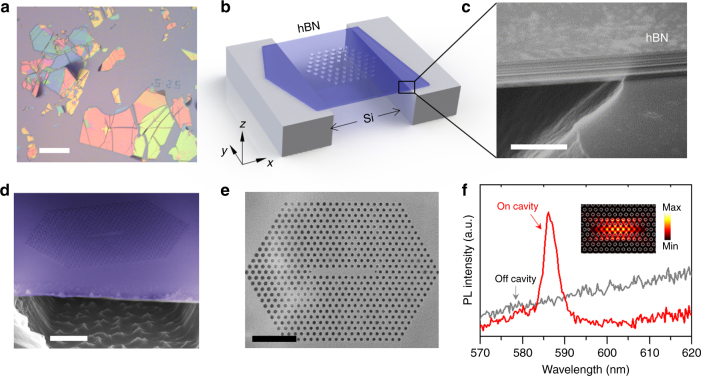
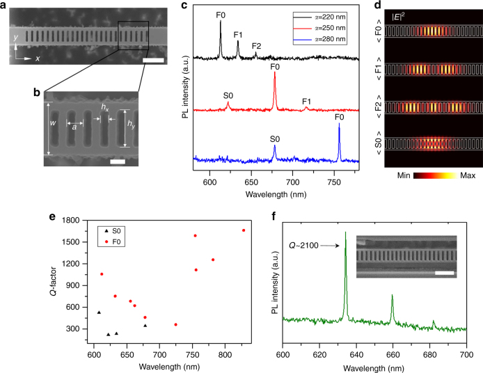
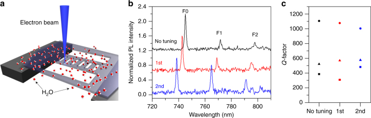
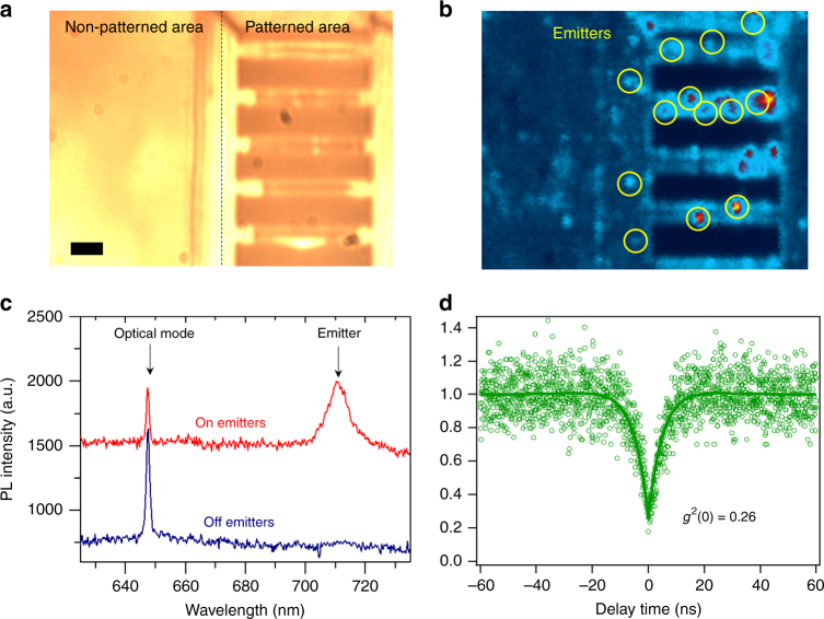
Development of scalable quantum photonic technologies requires on-chip integration of photonic components. Recently, hexagonal boron nitride (hBN) has emerged as a promising platform, following reports of hyperbolic phonon-polaritons and optically stable, ultra-bright quantum emitters. However, exploitation of hBN in scalable, on-chip nanophotonic circuits and cavity quantum electrodynamics (QED) experiments requires robust techniques for the fabrication of high-quality optical resonators. In this letter, we design and engineer suspended photonic crystal cavities from hBN and demonstrate quality (Q) factors in excess of 2000. Subsequently, we show deterministic, iterative tuning of individual cavities by direct-write EBIE without significant degradation of the Q-factor. The demonstration of tunable cavities made from hBN is an unprecedented advance in nanophotonics based on van der Waals materials. Our results and hBN processing methods open up promising avenues for solid-state systems with applications in integrated quantum photonics, polaritonics and cavity QED experiments.


Conflict of interest statement

The authors declare no competing interests.

Figures

Fig. 1
Fig. 1
Free-standing hexagonal boron nitride 2D photonic crystal cavities. a Optical microscope image of exfoliated hBN crystals on a silicon substrate. The scale bar corresponds to 50 µm. b Schematic of a free-standing hBN cavity on a trenched silicon substrate. c SEM image of the hBN showing the layered structure. The scale bar corresponds to 500 nm. d false color SEM image (45°) of a free-standing hBN photonic crystal cavity fabricated using a combination of RIE and EBIE. The scale bar corresponds to 2 µm. e Top view of a 2D photonic crystal cavity. The scale bar corresponds to 2 µm. f Photoluminescence spectra with a laser exciting the cavity mode (red) compared with an off-cavity excitation (gray). The inset depicts the electric field intensity profile of the fundamental mode for the cavity calculated using 3D FDTD
Fig. 2
Fig. 2
Optical analysis of one dimensional (1D) hBN photonic crystal cavities. a SEM image of a 1D ladder PCC with 25 rectangular air holes. The scale bar is 1 µm. b magnified view showing the geometrical parameters; width (w), lattice constant (a), air hole width (hx) and air hole height (hy). The cavity was fabricated using a combination of RIE and EBIE. The scale bar corresponds to 200 nm. c Photoluminescence spectra of different 1D ladder PCCs in the same hBN crystal with varying lattice constants of 220 nm (black), 250 nm (red), and 280 nm (blue), respectively. F0, F1, and F2 mark the position of the zeroth, first, and second order mode from the first dielectric band. S0 marks the position of the zeroth order from the second dielectric band mode. d 3D FDTD simulation result showing field profiles of the measured optical modes. e Experimentally obtained Q-factors of various 1D PCCs fabricated from hBN. f PL spectrum of a 1D cavity fabricated by focused ion beam milling, showing a high Q (~ 2100) mode in the visible spectral range. The inset is an SEM image of the cavity and the scale bar corresponds to 1 µm
Fig. 3
Fig. 3
Tuning of a 1D nanobeam cavity using direct-write, maskless EBIE. a Schematic of the etch process in which a focused electron beam (blue) is scanned along the outer sidewalls of the nanobeam cavity to induce the etch reaction in the presence of water molecules. b Photoluminescence (PL) spectra of a 1D photonic cavity before tuning (black), and after the first (red) and second (blue) tuning steps were performed by EBIE. c Q-factor of the F0 (circles) and F1 (triangles) modes measured immediately after fabrication (black), and after the first (red), and second (blue) tuning steps
Fig. 4
Fig. 4
Generation of single photon emitters within the hBN cavities. a optical microscope image of the analyzed area comparing an unprocessed site (left), with a processed site (right) that contains several 1D nanobeam cavities. The scale bar corresponds to 1 µm. b corresponding Photoluminescence map of this region. Positions of quantum emitters are indicated by yellow circles c PL spectra from two regions of the same cavity showing an optical mode only (blue) and the combination of an optical mode and an emitter (red). d Measured g2(τ) curve obtained from this emitter

References

    1. Majumdar A, Rundquist A, Bajcsy M, Vučković J. Cavity quantum electrodynamics with a single quantum dot coupled to a photonic molecule. Phys. Rev. B. 2012;86:045315. doi: 10.1103/PhysRevB.86.045315. - DOI
    1. Sekoguchi H, Takahashi Y, Asano T, Noda S. Photonic crystal nanocavity with a Q-factor of ~9 million. Opt. Express. 2014;22:916–924. doi: 10.1364/OE.22.000916. - DOI - PubMed
    1. Shen Y, et al. Deep learning with coherent nanophotonic circuits. Nat. Photonics. 2017;11:441. doi: 10.1038/nphoton.2017.93. - DOI
    1. Zhong T, Kindem JM, Miyazono E, Faraon A. Nanophotonic coherent light–matter interfaces based on rare-earth-doped crystals. Nat. Commun. 2015;6:8206. doi: 10.1038/ncomms9206. - DOI - PMC - PubMed
    1. Faraon A, Barclay PE, Santori C, Fu KMC, Beausoleil RG. Resonant enhancement of the zero-phonon emission from a colour centre in a diamond cavity. Nat. Photonics. 2011;5:301–305. doi: 10.1038/nphoton.2011.52. - DOI

Publication types