. 2018 Jul 16;9(1):2737.
doi: 10.1038/s41467-018-05155-y.

Intrinsically ionic conductive cellulose nanopapers applied as all solid dielectrics for low voltage organic transistors

Affiliations

Intrinsically ionic conductive cellulose nanopapers applied as all solid dielectrics for low voltage organic transistors

Shilei Dai et al. Nat Commun. .

Abstract

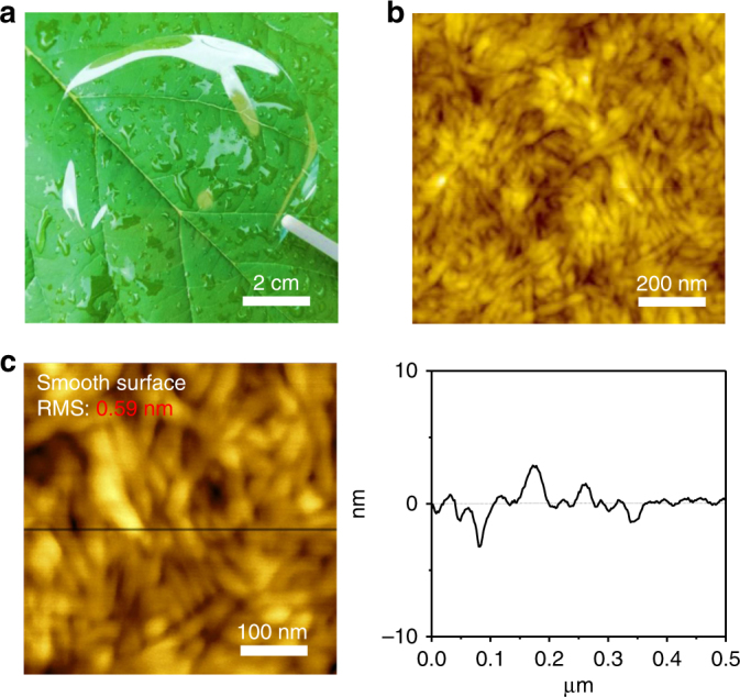
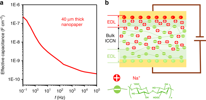
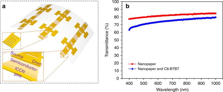
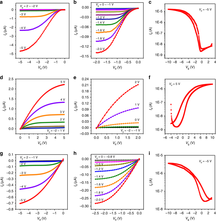
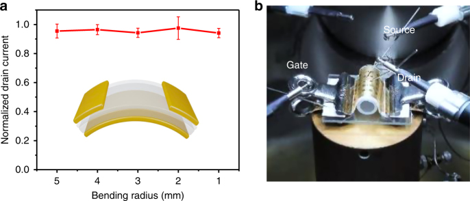
Biodegradability, low-voltage operation, and flexibility are important trends for the future organic electronics. High-capacitance dielectrics are essential for low-voltage organic field-effect transistors. Here we report the application of environmental-friendly cellulose nanopapers as high-capacitance dielectrics with intrinsic ionic conductivity. Different with the previously reported liquid/electrolyte-gated dielectrics, cellulose nanopapers can be applied as all-solid dielectrics without any liquid or gel. Organic field-effect transistors fabricated with cellulose nanopaper dielectrics exhibit good transistor performances under operation voltage below 2 V, and no discernible drain current change is observed when the device is under bending with radius down to 1 mm. Interesting properties of the cellulose nanopapers, such as ionic conductivity, ultra-smooth surface (~0.59 nm), high transparency (above 80%) and flexibility make them excellent candidates as high-capacitance dielectrics for flexible, transparent and low-voltage electronics.


Conflict of interest statement

The authors declare no competing interests.

Figures

Fig. 1
Fig. 1
Photograph and AFM characterization of ICCN. a Photograph of a highly transparent 40 μm-thick ICCN. b AFM image of a ICCN. c AFM line scan of a ICCN, shows ultra-smooth surface with RMS of ~0.59 nm
Fig. 2
Fig. 2
Chemical structure, FTIR and XPS analysis of ICCNs. a The chemical structure of ICCNs pretreated with TEMPO. The FTIR spectra (b) and XPS spectrum (c) of a 40 μm-thick ICCN
Fig. 3
Fig. 3
Frequency dependent effective capacitance of 40 μm thick ICCNs. a Frequency-dependent effective capacitance (C-f) of a 40 μm-thick ICCN measured in a metal/insulator/metal (Au/ICCN/Au) structure. b Schematic diagram demonstrates the formation of EDL in ICCNs under the action of electric field
Fig. 4
Fig. 4
Schematic of transparent OFET based on ICCN. a Schematic illustration of the ICCN based OFETs with a bottom gate top contact architecture. b Optical transmittance of a 40 μm-thick ICCN and an ICCN/C8-BTBT composite film at different wavelengths
Fig. 5
Fig. 5
Electrical characteristics of ICCNs based OFETs. a, b IdVd curves and c transfer characteristics curves (Id–Vg) of a p-channel C8-BTBT OFET. d, e Id−Vd curves and f transfer characteristics curves (Id−Vg) of a n-channel NTCDI-F15 OFET. g, h Id−Vd curves and i transfer characteristics curves (Id−Vg) of a PQT-12 OFET
Fig. 6
Fig. 6
Bending tests on flexible OFETs. a Normalized maximum drain current at Vg of −6 V and Vd of −5 V (normalized to the initial drain current measured in the flat state) as a function of the bending radius. Error bars represent standard errors from five times independent tests of a device. b The picture depicts implementation of this bending test
Fig. 7
Fig. 7
Organic complementary inverter on ICCN dielectrics. a Image of an organic complementary inverter and its simplified circuit diagram. b Output voltage and c gain as a function of the input voltage with supply voltage step between 2−5 V. The input voltage was swept from −2 to 4 V

References

    1. Robinson BH. E-waste: an assessment of global production and environmental impacts. Sci. Total Environ. 2009;408:183–191. doi: 10.1016/j.scitotenv.2009.09.044. - DOI - PubMed
    1. Liu Q, et al. Chromosomal aberrations and DNA damage in human populations exposed to the processing of electronics waste. Environ. Sci. Pollut. Res. Int. 2009;16:329–338. doi: 10.1007/s11356-008-0087-z. - DOI - PubMed
    1. Lei T, et al. Biocompatible and totally disintegrable semiconducting polymer for ultrathin and ultralightweight transient electronics. Proc. Natl Acad. Sci. USA. 2017;114:5107–5112. doi: 10.1073/pnas.1701478114. - DOI - PMC - PubMed
    1. Zhu H, et al. Wood-derived materials for green electronics, biological devices, and energy applications. Chem. Rev. 2016;116:9305–9374. doi: 10.1021/acs.chemrev.6b00225. - DOI - PubMed
    1. Irimia-Vladu M. “Green” electronics: biodegradable and biocompatible materials and devices for sustainable future. Chem. Soc. Rev. 2014;43:588–610. doi: 10.1039/C3CS60235D. - DOI - PubMed

Publication types

LinkOut - more resources