. 2018 Jun 6;5(8):1800496.
doi: 10.1002/advs.201800496. eCollection 2018 Aug.

Single-Step Selective Laser Writing of Flexible Photodetectors for Wearable Optoelectronics

Affiliations

Single-Step Selective Laser Writing of Flexible Photodetectors for Wearable Optoelectronics

Jianing An et al. Adv Sci (Weinh). .

Abstract

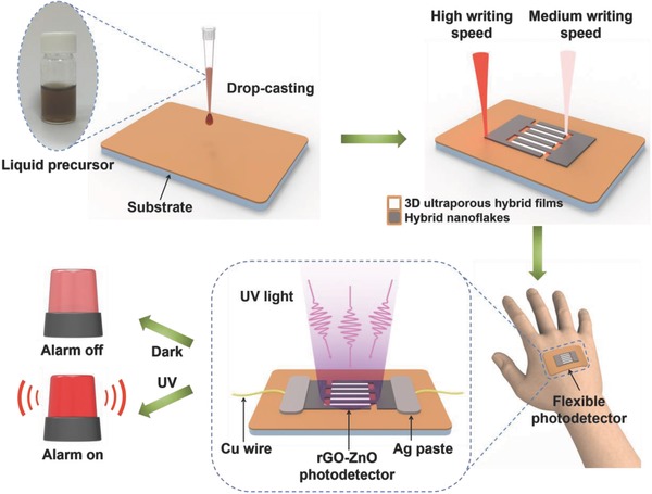
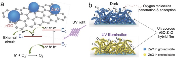
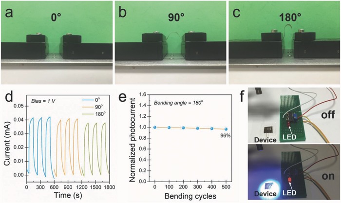
The increasing demand for wearable optoelectronics in biomedicine, prosthetics, and soft robotics calls for innovative and transformative technologies that permit facile fabrication of compact and flexible photodetectors with high performance. Herein, by developing a single-step selective laser writing strategy that can finely tailor material properties through incident photon density control and lead to the formation of hierarchical hybrid nanocomposites, e.g., reduced graphene oxide (rGO)-zinc oxide (ZnO), a highly flexible and all rGO-ZnO hybrid-based photodetector is successfully constructed. The device features 3D ultraporous hybrid films with high photoresponsivity as the active detection layer, and hybrid nanoflakes with superior electrical conductivity as interdigitated electrodes. Benefitting from enhanced photocarrier generation because of the ultraporous film morphology, efficient separation of electron-hole pairs at rGO-ZnO heterojunctions, and fast electron transport by highly conductive rGO nanosheets, the photodetector exhibits high, linear, and reproducible responsivities to a wide range of ultraviolet (UV) intensities. Furthermore, the excellent mechanical flexibility and robustness enable the photodetector to be conformally attached to skin, thus intimately monitoring the exposure dosage of human body to UV light for skin disease prevention. This study advances the fabrication of flexible optoelectronic devices with reduced complexity, facilitating the integration of wearable optoelectronics and epidermal systems.

Keywords: flexible photodetectors; graphene hybrids; hierarchical morphology; single‐step selective laser writing; wearable optoelectronics.


Figures

Figure 1
Figure 1
Schematic illustration of the preparation of all rGO–ZnO hybrid‐based photodetector through a single‐step FsLDW process by selecting suitable writing speed for respectively patterning the interdigitated electrodes and the active detection layer. The flexible photodetector can be used for human skin protection.
Figure 2
Figure 2
Morphology and chemical composition modulation of the rGO–ZnO heterostructures by the writing speed. a–c) SEM images (top surface) of the hybrids produced under low, medium, and high writing speeds, respectively. The insets are top views at a higher magnification. d–f) Cross‐section SEM images of the nanostructures synthesized under low, medium, and high writing speeds, respectively. Their corresponding EDS element (C, O, and Zn) mapping profiles are respectively displayed in panels (g)–(i), scale bar: 10 µm. j) EDS spectra of the three rGO–ZnO hybrids, the insets present the element analysis in weight and atomic percentage.
Figure 3
Figure 3
Characterizations of the rGO–ZnO hybrids. a) XPS C1s spectra of GO and rGO–ZnO hybrids. b) XPS Zn2p spectra of rGO–ZnO hybrids. c) XRD patterns of GO and rGO–ZnO hybrids. d) Raman spectra of GO and rGO–ZnO hybrids. e) Sheet resistances of the rGO–ZnO films produced at three levels of writing speed. f) Photoresponse behaviors of the three rGO–ZnO hybrids. The hybrid‐M generates the largest photocurrent.
Figure 4
Figure 4
Interdigitated photodetector fabricated by the single‐step FsLDW and the photoresponse performances. a) An optical image of the as‐written interdigitated photodetector, an enlarged SEM image indicates the active detection layer and the electrode. b) The photocurrent and the responsivity as a function of the channel length. c) Time‐resolved photocurrent responses of the photodetector (channel length of 40 µm) to different UV illumination intensities at a bias of 1 V. d) The dependence of photocurrent on incident light intensity. e) Time response of the same device under UV illumination with the light intensity of 20.03 mW cm−2.
Figure 5
Figure 5
Photoresponse mechanism of the ultraporous all rGO–ZnO photodetector. a) Energy band diagram of the rGO–ZnO hybrid. E C and E V represent the conduction band and valence band of ZnO, respectively; E F represents the Fermi level of rGO. b) Schematic model of the photodetection mechanism of the 3D ultraporous rGO–ZnO hybrid film.
Figure 6
Figure 6
Flexible photodetector and its application as a photoswitch. a–c) Optical images of a flexible photodetector with the bending angle of 0°, 90°, and 180°, respectively. d) Time‐resolved photoresponse curves of the device at different bending angles. e) Normalized photocurrent of the flexible photodetector with respect to the bending–unbending cycles at 1 V bias, the bending angle is 180°. f) Optical images of the photoswitch triggering a red LED upon UV illumination. Upper panel: before UV illumination (LED in the “off” state); lower panel: after UV illumination (LED in the “on” state).

References

    1. a) Sang L., Liao M., Sumiya M., Sensors 2013, 13, 10482; - PMC - PubMed
    2. b) Tian W., Zhang C., Zhai T., Li S.‐L., Wang X., Liu J., Jie X., Liu D., Liao M., Koide Y., Golberg D., Bando Y., Adv. Mater. 2014, 26, 3088; - PubMed
    3. c) Nasiri N., Bo R., Wang F., Fu L., Tricoli A., Adv. Mater. 2015, 27, 4336; - PubMed
    4. d) Araki H., Kim J., Zhang S., Banks A., Crawford K. E., Sheng X., Gutruf P., Shi Y., Pielak R. M., Rogers J. A., Adv. Funct. Mater. 2017, 27, 1604465;
    5. e) Zheng W., Lin R., Ran J., Zhang Z., Ji X., Huang F., ACS Nano 2018, 12, 425. - PubMed
    1. a) Kim J., Salvatore G. A., Araki H., Chiarelli A. M., Xie Z., Banks A., Sheng X., Liu Y., Lee J. W., Jang K.‐I., Heo S. Y., Cho K., Luo H., Zimmerman B., Kim J., Yan L., Feng X., Xu S., Fabiani M., Gratton G., Huang Y., Paik U., Rogers J. A., Sci. Adv. 2016, 2, e1600418; - PMC - PubMed
    2. b) Jin Z., Gao L., Zhou Q., Wang J., Sci. Rep. 2014, 4, 4268. - PMC - PubMed
    1. a) Bao Z., Chen X., Adv. Mater. 2016, 28, 4177; - PubMed
    2. b) Liu Y., Pharr M., Salvatore G. A., ACS Nano 2017, 11, 9614. - PubMed
    1. Zhan Z., An J., Wei Y., Tran V. T., Du H., Nanoscale 2017, 9, 965. - PubMed
    1. Liu N., Tian H., Schwartz G., Tok J. B. H., Ren T.‐L., Bao Z., Nano Lett. 2014, 14, 3702. - PubMed

LinkOut - more resources