doi: 10.1364/OE.26.021887.
Microscope calibration using laser written fluorescence
- PMID: 30130891
- PMCID: PMC6238825
- DOI: 10.1364/OE.26.021887
Item in Clipboard
Microscope calibration using laser written fluorescence
Opt Express.
.
Abstract
There is currently no widely adopted standard for the optical characterization of fluorescence microscopes. We used laser written fluorescence to generate two- and three-dimensional patterns to deliver a quick and quantitative measure of imaging performance. We report on the use of two laser written patterns to measure the lateral resolution, illumination uniformity, lens distortion and color plane alignment using confocal and structured illumination fluorescence microscopes.
Figures
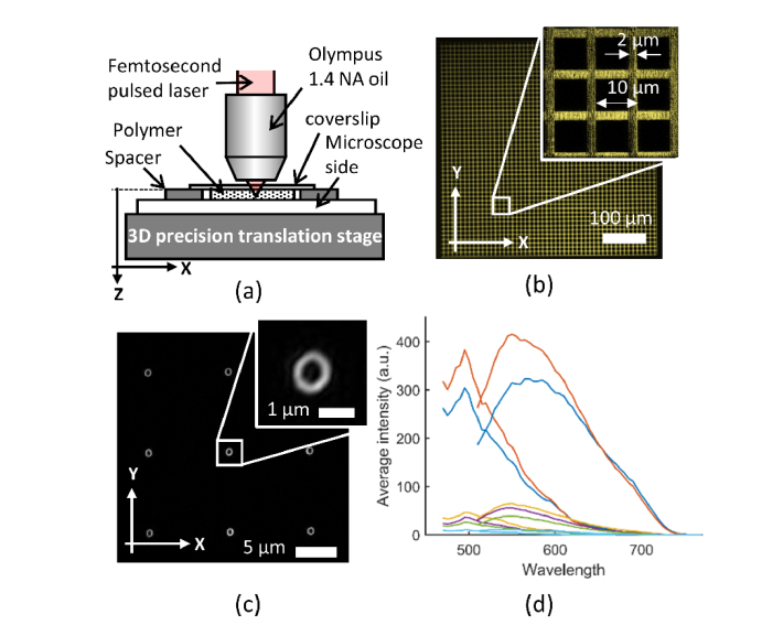
(a) Fabrication of the features within the polymer substrate using a pulsed IR laser. (b) The fluorescent grid target showing with the microstructure from the laser writing process, and magnified in the inset. (c) SIM images of individual fabrication features on a 10 μm pitch. (d) Excitation and emission fluorescence spectra for the laser fabricated regions. Wavelength is in nm. The fabrication powers used to produce the spectra are (according to line colour) orange = 8.0 nJ, dark blue = 6.8 nJ, yellow = 5.7 nJ, purple = 4.7 nJ, green = 3.8 nJ, light blue = background fluorescence.

XY section through the confocal data stack of the 8 × 8 × 3 array. The dashed line indicates the location of the XZ section shown below. Z increases with distance into the sample. Scale bars: 10 μm.

SIM images of individual features fabricated using a range of pulse energies and repetitions. (a)-(c): five pulses, with energies of: 8 nJ (a), 4.7 nJ (b) and 3.8 nJ (c). (d)-(f) single pulse, with energies of: 5.7 nJ (d), 4.7 nJ (e), 3.8 nJ (f). Image brightness has been adjusted for clarity.

Relationship between shell diameter, shell thickness, and fabrication parameters for the SIM images shown in Fig. 3. The plots indicate a linear relationship between shell diameter and pulse energy, whilst the apparent shell thickness remains independent of pulse energy.

Line transects across SIM images of the fluorescent shells shown in Fig. 3. The line profiles correspond to features fabricated with the following parameters: 5 × 8 nJ (green) 5 × 4.7 nJ (blue) 5 × 3.8 nJ (yellow), 1 × 5.7 nJ (grey), 1 × 4.7 nJ (orange), 1 × 3.8 nJ (blue). The dashed blue line shown the profile of a 100 nm fluorescent bead captured on the same microscope.

Images of fluorescent features taken on a Zeiss Airyscan confocal microscope operating in standard confocal mode. (a)-(d): five pulses, with energies of: 7.4 nJ (a), 6 nJ (b) 5.4 nJ (c) and 4.8 nJ (e)-(f) single pulse, with energies of: 7.4 nJ (e), 4.2 nJ (f). Image brightness has been adjusted for clarity.

Line transects through fluorescent shells shown in Fig. 6. The dashed blue line is an average line profile through images of a 100 nm bead taken on the same microscope. The black dashed line indicates the Rayleigh limit which determines the condition for the separation of the two sides of the fluorescent shell to be distinguishable.

(a) Raw image of the fluorescent grid using a 40X objective lens taken on a Zeiss Axioplan 2. (b) The Fourier transform of (a) with the zero order blocked to better visualise location of higher orders.(c) Inverse Fourier transform of region passing through red spatial filter in (b). (d) The wrapped phase angle of the signal passing through the green spatial filer in (b). Scale bar: 100 μm.

Demonstrating the accuracy of the distortion correction algorithm. (a): An ideal grid was warped using the MATLAB imwarp function before being used as input into the distortion correction algorithm. (b) Details from the overlap of the ideal grid (white) on the distortion corrected grid (red). Each tile corresponds to the numbered regions highlighted in (a). (c) Pixel shift map showing the size and direction of the unwarping within each region to recover the original grid pattern. (d) Details of the pixel shift map, with tiles corresponding to the numbered regions in (c).

Multi-channel images of a single layer of the 8 × 8 × 3 array, with a 2 × 2 detail shown inset. Excitation wavelengths (a)-(c) are: 405 nm, 488 nm and 561 nm, with detection bandwidths 430-470 nm, 500-540 nm and 570-620 nm respectively. (d) An image fusing the different colour planes into a single image showing the sub-pixel colour alignment. Images were acquired on an Olympus FV3000.
References
-
- “Editorial, “Keeping up standards,” Nat. Photonics 12(3), 117 (2018).
-
- Horstmeyer R., Heintzmann R., Popescu G., Waller L., Yang C., “Standardizing the resolution claims for coherent microscopy,” Nat. Photonics 10(2), 68–71 (2016).10.1038/nphoton.2015.279 - DOI
-
- Bellec M., Royon A., Bourhis K., Choi J., Bousquet B., Treguer M., Cardinal T., Videau J.-J., Richardson M., Canioni L., “3D Patterning at the Nanoscale of Fluorescent Emitters in Glass,” J. Phys. Chem. C 114(37), 15584–15588 (2010).10.1021/jp104049e - DOI
Grants and funding
LinkOut - more resources
Full Text Sources
Other Literature Sources