Variable optofluidic slit aperture
- PMID: 30167111
- PMCID: PMC6059840
- DOI: 10.1038/lsa.2016.5
Variable optofluidic slit aperture
Abstract
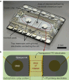
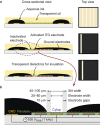
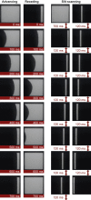
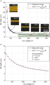
The shape of liquid interfaces can be precisely controlled using electrowetting, an actuation mechanism which has been widely used for tunable optofluidic micro-optical components such as lenses or irises. We have expanded the considerable flexibility inherent in electrowetting actuation to realize a variable optofluidic slit, a tunable and reconfigurable two-dimensional aperture with no mechanically moving parts. This optofluidic slit is formed by precisely controlled movement of the liquid interfaces of two highly opaque ink droplets. The 1.5 mm long slit aperture, with controllably variable discrete widths down to 45 µm, may be scanned across a length of 1.5 mm with switching times between adjacent slit positions of less than 120 ms. In addition, for a fixed slit aperture position, the width may be tuned to a minimum of 3 µm with high uniformity and linearity over the entire slit length. This compact, purely fluidic device offers an electrically controlled aperture tuning range not achievable with extant mechanical alternatives of a similar size.
Keywords: electrowetting on dielectrics (EWOD); optofluidics; scanning slit aperture; tunable.
Figures


Similar articles
-
Optofluidic lens based on electrowetting liquid piston.Sci Rep. 2019 Sep 10;9(1):13062. doi: 10.1038/s41598-019-49560-9. Sci Rep. 2019. PMID: 31506551 Free PMC article.
-
Optofluidic router based on tunable liquid-liquid mirrors.Lab Chip. 2014 Feb 21;14(4):737-43. doi: 10.1039/c3lc51148k. Epub 2013 Nov 29. Lab Chip. 2014. PMID: 24287814
-
Electrowetting-driven solar indoor lighting (e-SIL): an optofluidic approach towards sustainable buildings.Lab Chip. 2018 Jun 12;18(12):1725-1735. doi: 10.1039/c8lc00319j. Lab Chip. 2018. PMID: 29726880
-
Recent Developments in Optofluidic Lens Technology.Micromachines (Basel). 2016 Jun 10;7(6):102. doi: 10.3390/mi7060102. Micromachines (Basel). 2016. PMID: 30404276 Free PMC article. Review.
-
Electrically Tunable Lenses for Imaging and Light Manipulation.Micromachines (Basel). 2023 Jan 26;14(2):319. doi: 10.3390/mi14020319. Micromachines (Basel). 2023. PMID: 36838021 Free PMC article. Review.
Cited by
-
Adaptive aberration correction using an electrowetting array.Appl Phys Lett. 2023 Feb 20;122(8):081102. doi: 10.1063/5.0133473. Epub 2023 Feb 21. Appl Phys Lett. 2023. PMID: 36846091 Free PMC article.
-
Liquid Core ARROW Waveguides: A Promising Photonic Structure for Integrated Optofluidic Microsensors.Micromachines (Basel). 2016 Mar 11;7(3):47. doi: 10.3390/mi7030047. Micromachines (Basel). 2016. PMID: 30407419 Free PMC article. Review.
-
A Novel Self-Activated Mechanism for Stable Liquid Transportation Capable of Continuous-Flow and Real-time Microfluidic PCRs.Micromachines (Basel). 2019 May 28;10(6):350. doi: 10.3390/mi10060350. Micromachines (Basel). 2019. PMID: 31141967 Free PMC article.
-
Holographic detection of nanoparticles using acoustically actuated nanolenses.Nat Commun. 2020 Jan 16;11(1):171. doi: 10.1038/s41467-019-13802-1. Nat Commun. 2020. PMID: 31949134 Free PMC article.
-
High extinction ratio, low insertion loss, optical switch based on an electrowetting prism.Opt Express. 2020 Mar 2;28(5):5991-6001. doi: 10.1364/OE.381565. Opt Express. 2020. PMID: 32225857 Free PMC article.
References
-
- Czerny M, Turner A. Über den Astigmatismus bei Spiegelspektrometern. Zeitschrift für Phys 1930; 61: 792–797.
-
- Lerner JM. Imaging spectrometer fundamentals for researchers in the biosciences – a tutorial. Cytom Part A 2006; 69A: 712–734. - PubMed
-
- Chronis N, Okandan M, Baker M, Lee LP. A 2-D translational pinhole formed by two orthogonally moving micro-slits. Digest of Technical Papers – The 13th International Conference on Solid-State Sensors, Actuators and Microsystems, Transducers ’05; 5–9 June 2005; Seoul, South Korea; 2005, pp. 1022–1025.
-
- Vuilleumier R, Kraiczek K. Variable-entrance-slit system for precision spectrophotometers. Sensor Actuat A Phys 1995; 50: 87–91.
LinkOut - more resources
Full Text Sources
Other Literature Sources

