Review
. 2016 Mar 11;5(3):e16040.
doi: 10.1038/lsa.2016.40. eCollection 2016 Mar.

Optical second-harmonic generation measurement for probing organic device operation

Affiliations
Review

Optical second-harmonic generation measurement for probing organic device operation

Takaaki Manaka et al. Light Sci Appl. .

Abstract

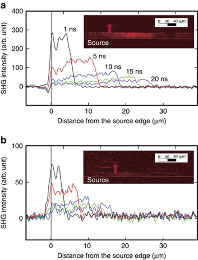
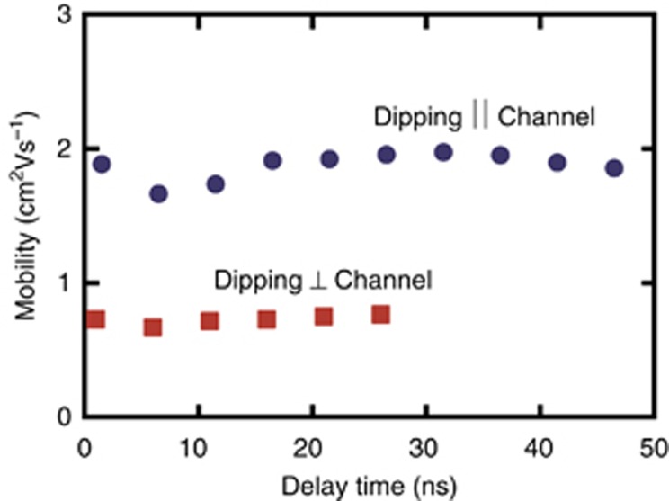
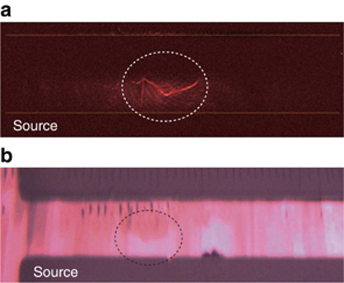
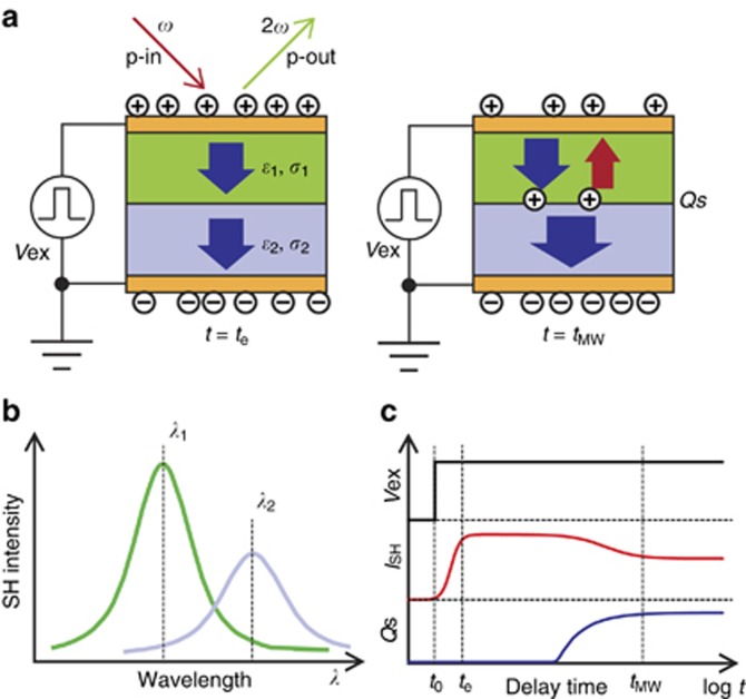
We give a brief overview of the electric-field induced optical second-harmonic generation (EFISHG) technique that has been used to study the complex behaviors of organic-based devices. By analyzing EFISHG images of organic field-effect transistors, the in-plane two-dimensional distribution of the electric field in the channel can be evaluated. The susceptibility tensor of the organic semiconductor layer and the polarization of the incident light are considered to determine the electric field distribution. EFISHG imaging can effectively evaluate the distribution of the vectorial electric field in organic films by selecting a light polarization. With the time-resolved technique, measurement of the electric field originating from the injected carriers allows direct probing of the carrier motion under device operation, because the transient change of the electric field distribution reflects the carrier motion. Some applications of the EFISHG technique to organic electronic devices are reviewed.

Keywords: electric field; optical second-harmonic generation; semiconductor device.


Conflict of interest statement

The authors declare no conflict of interest.

Figures

Figure 1
Figure 1
(a) Optical setup for the microscopic SHG measurement. The light source was a femtosecond optical parametric amplifier pumped by a Ti:Sapphire-regenerative (regen.) amplifier (amp.) system. (b) Device structure and the electrical connection of the TRM-SHG measurement. (c) Optical geometry for the SHG measurement. CCD, charge-coupled device; DUT, device under test; IR, infra-red; OS, organic semiconductor.
Figure 2
Figure 2
(a) SHG image of the channel in C60 FET under positive pulse application to the source and the drain electrodes. (b) EFISHG profile obtained by taking a line scan across the channel from the SHG image. (c) Electric field distribution obtained from the SHG distribution.
Figure 3
Figure 3
(a) Microscopic image of the edge of the electrode. Arrows schematically show the direction of the electric field. (b) Microscopic SHG image near the edge of the electrode under a parallel polarizer condition. (c) Microscopic SHG image near the edge of the electrode under a crossed polarizer condition (SHG intensity was 10 times magnified).
Figure 4
Figure 4
Transient SHG intensity distribution along the FET channel with different delay times. (a) Device in which the dipping direction is parallel to the source–drain direction. (b) Device in which the dipping direction is perpendicular to the source–drain direction. Insets are the actual SHG images from the OFET channel.
Figure 5
Figure 5
Transient carrier mobility of the samples with different dipping directions calculated by using Equation (7) at different delay times.
Figure 6
Figure 6
(a) Polarized microscopic image of the circular Au electrode. (b) TRM-SHG images from TIPS-pentacene single crystalline grain covered with a circular-shaped electrode at a delay time of 20 ns.
Figure 7
Figure 7
(a) Bright line observed in the SHG image from the channel of TIPS-pentacene FET (see inside a dashed circle). (b) Polarized microscope image around the same area.
Figure 8
Figure 8
(a) Experimental configuration of the SHG measurement for OLED. (b) Schematic image of the SHG spectrum of double-layered structure. (c) Transient SHG response and the accumulated carriers with respect to the voltage pulse. SH, second-harmonic.

References

    1. Zhou LS, Wanga A, Wu SC, Sun J, Park S et al. All-organic active matrix flexible display. Appl Phys Lett 2006; 88: 083502.
    1. Lodha A, Singh R. Prospects of manufacturing organic semiconductor-based integrated circuits. IEEE Trans Semi Manu 2001; 14: 281–296.
    1. Nonnenmacher M, O'Boyle MP, Wickramasinghe HK. Kelvin probe force microscopy. Appl Phys Lett 1991; 58: 2921–2923.
    1. Vatel O, Tanimoto M. Kelvin probe force microscopy for potential distribution measurement of semiconductor devices. J Appl Phys 1995; 77: 2358–2362.
    1. Kikukawa A, Hosaka S, Imura R. Silicon pn junction imaging and characterizations using sensitivity enhanced Kelvin probe force microscopy. Appl Phys Lett 1995; 66: 3510–3512.

LinkOut - more resources