Optically controlled magnetic-field etching on the nano-scale
- PMID: 30167154
- PMCID: PMC6059895
- DOI: 10.1038/lsa.2016.54
Optically controlled magnetic-field etching on the nano-scale
Abstract
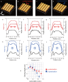
Electric and magnetic fields play an important role in both chemical and physical reactions. However, since the coupling efficiency between magnetic fields and electrons is low in comparison with that between electric fields and electrons in the visible wavelength region, the magnetic field is negligible in photo-induced reactions. Here, we performed photo-etching of ZrO2 nano-stripe structures, and identified an etching-property polarisation dependence. Specifically, the etching rate and etched profiles depend on the structure width. To evaluate this polarisation-dependent etching, we performed numerical calculations using a finite-difference time-domain method. Remarkably, the numerical results revealed that the polarisation-dependent etching properties were determined by the magnetic field distributions, rather than the electric field distributions. As nano-scale structures induce a localised magnetic field, the discovery of this etching dependence on the magnetic field is expected to introduce a new perspective on advanced nano-scale structure fabrication.
Keywords: nano-scale; near-field etching; optically controlled magnetic-field interaction.
Figures


Similar articles
-
Controlled Patterning of Vertical Silicon Structures Using Polymer Lithography and Wet Chemical Etching.J Nanosci Nanotechnol. 2015 Jun;15(6):4522-9. doi: 10.1166/jnn.2015.9780. J Nanosci Nanotechnol. 2015. PMID: 26369075
-
Experimental demonstration of linear and spinning Janus dipoles for polarisation- and wavelength-selective near-field coupling.Light Sci Appl. 2019 Jun 5;8:52. doi: 10.1038/s41377-019-0162-x. eCollection 2019. Light Sci Appl. 2019. PMID: 31231518 Free PMC article.
-
Anti-reflectance investigation of a micro-nano hybrid structure fabricated by dry/wet etching methods.Sci Rep. 2018 May 18;8(1):7863. doi: 10.1038/s41598-018-26234-6. Sci Rep. 2018. PMID: 29777186 Free PMC article.
-
Electric field-induced effects on neuronal cell biology accompanying dielectrophoretic trapping.Adv Anat Embryol Cell Biol. 2003;173:III-IX, 1-77. doi: 10.1007/978-3-642-55469-8. Adv Anat Embryol Cell Biol. 2003. PMID: 12901336 Review.
-
Numerical dosimetry ELF: accuracy of the method, variability of models and parameters, and the implication for quantifying guidelines.Health Phys. 2007 Jun;92(6):521-30. doi: 10.1097/01.HP.0000251249.00507.ca. Health Phys. 2007. PMID: 17495652 Review.
Cited by
-
Synthesis of silver nanostructure on gold nanoparticle using near field assisted second harmonic generation.Sci Rep. 2021 Mar 11;11(1):5642. doi: 10.1038/s41598-021-84944-w. Sci Rep. 2021. PMID: 33707508 Free PMC article.
-
Angstrom-scale flatness using selective nanoscale etching.Beilstein J Nanotechnol. 2017 Oct 18;8:2181-2185. doi: 10.3762/bjnano.8.217. eCollection 2017. Beilstein J Nanotechnol. 2017. PMID: 29114444 Free PMC article.
-
The Coupling Effects of Surface Plasmon Polaritons and Magnetic Dipole Resonances in Metamaterials.Nanoscale Res Lett. 2017 Nov 9;12(1):586. doi: 10.1186/s11671-017-2350-z. Nanoscale Res Lett. 2017. PMID: 29124431 Free PMC article.
References
-
- Dürig U, Pohl DW, Rohner F. Near‐field optical‐scanning microscopy. J Appl Phys 1986; 59: 3318–3327.
-
- Betzig E, Chichester RJ. Single molecules observed by near-field scanning optical microscopy. Science 1993; 262: 1422–1425. - PubMed
-
- Matsuda K, Saiki T, Nomura S, Mihara M, Aoyagi Y et al. Near-field optical mapping of exciton wave functions in a GaAs quantum dot. Phys Rev Lett 2003; 91: 177401. - PubMed
-
- Yano T, Verma P, Saito Y, Ichimura T, Kawata S. Pressure-assisted tip-enhanced Raman imaging at a resolution of a few nanometres. Nat Photonics 2009; 3: 473–477.
-
- Shalaev VM. Optical negative-index metamaterials. Nat Photonics 2007; 1: 41–48.
LinkOut - more resources
Full Text Sources
Other Literature Sources
Research Materials

