Review
. 2016 Aug 12;5(8):e16133.
doi: 10.1038/lsa.2016.133. eCollection 2016 Aug.

Ultrafast laser processing of materials: from science to industry

Affiliations
Review

Ultrafast laser processing of materials: from science to industry

Mangirdas Malinauskas et al. Light Sci Appl. .

Abstract

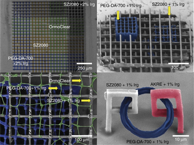
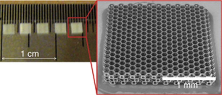
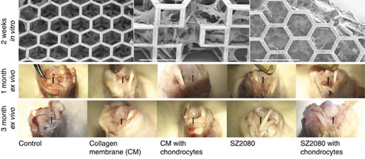
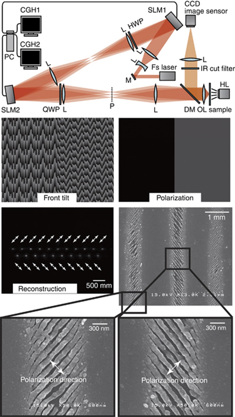
Processing of materials by ultrashort laser pulses has evolved significantly over the last decade and is starting to reveal its scientific, technological and industrial potential. In ultrafast laser manufacturing, optical energy of tightly focused femtosecond or picosecond laser pulses can be delivered to precisely defined positions in the bulk of materials via two-/multi-photon excitation on a timescale much faster than thermal energy exchange between photoexcited electrons and lattice ions. Control of photo-ionization and thermal processes with the highest precision, inducing local photomodification in sub-100-nm-sized regions has been achieved. State-of-the-art ultrashort laser processing techniques exploit high 0.1-1 μm spatial resolution and almost unrestricted three-dimensional structuring capability. Adjustable pulse duration, spatiotemporal chirp, phase front tilt and polarization allow control of photomodification via uniquely wide parameter space. Mature opto-electrical/mechanical technologies have enabled laser processing speeds approaching meters-per-second, leading to a fast lab-to-fab transfer. The key aspects and latest achievements are reviewed with an emphasis on the fundamental relation between spatial resolution and total fabrication throughput. Emerging biomedical applications implementing micrometer feature precision over centimeter-scale scaffolds and photonic wire bonding in telecommunications are highlighted.

Keywords: 3D structuring; biomedical applications; direct laser writing; functional microdevices; material processing; nonlinear light–matter interaction; ultrashort laser pulses.


Figures

Figure 1
Figure 1
Beam focusing approaches: (a) a beam is focused on the surface or volume of a material; (b) an fs-beam is focused on liquid and forms a light filament suitable for processing of transparent and opaque workpieces at different axial locations or curvature of the surface. Reproduced with permission from Ref. . JLPS. All rights reserved.
Figure 2
Figure 2
Tennant’s scaling: state-of-the-art of nanotechnology in 2003 for the resolution vs. throughput R=2.35 T2D (Ref. 27). Direct 3D laser writing for polymerization with T ≃ 109 μm3 h–1, Bragg grating recording by Bessel–Gauss fs-beam in glass, surface ripple formation on crystals/glasses are marked along with the Tennant’s law predictions rescaled for the 3D C × 106 μm3 h–1 with C=32.2 taken from the speed of protein production in ribosome (see text for details). The size of elliptical markers is representative of the resolution span; the current 22 nm node of modern CMOS lithography is marked by an arrow.
Figure 3
Figure 3
A cross-pivot hinge out of fused silica as a part of a mechanical structure. The images show the three crossed beams and the rounded corners at the location where the beams are connected to the main body. Note the high aspect ratio of the micromachining process. Reproduced with permission from Ref. . MDPI. All rights reserved.
Figure 4
Figure 4
Freeform 3D micro-optical elements fabricated by DLW: hybrid optical elements—aspheric and axicon lenses on a tip of optical fiber. Reproduced with permission from Ref. . JLPS. All rights reserved.
Figure 5
Figure 5
Optical vortex generating spiral waveplates. Smaller (a, b) and larger (c) cross-sections optical vortex generators. (a, b) SEM images of micro-plates made by point-by-point exposure (inset in b shows 3D construction of irradiation matrix). (c) Height scans at four locations of the step edge of the spiral plate; diameter of the plate was 60 μm. Reproduced with permission from Ref. . Copyright (2010), AIP Publishing LLC.
Figure 6
Figure 6
Coloration via slowing light. (a) SEM image of 3D woodpile architecture PhC in photoresist SZ2080, (b) optical microscopy image of several woodpile structures having different lattice parameters and exhibiting different structural color, (c) comparison between experimental optical reflectivity spectrum of the sample shown in a and numerically simulated reflectivity spectrum as well as photonic band diagram. Reproduced with permission from Ref. . JLPS. All rights reserved.
Figure 7
Figure 7
(a) A typical DLW STED exposure profile: red volume represents standard focusing exciting the material; green represents a phase mask-generated depletion (bottle beam); violet is the resulting modified volume (excitation is minimized by cutting the side and top-bottom lobes with a shaped depletion beam). (b) Using the same excitation conditions but increasing the depletion power, the feature size shrinks (from left to right, it is minimized from 220 nm down to 65 nm). (c, d) Magnified and full-scale image of 3D chiral polarizer structure fabricated employing simultaneous combination of dip-in and STED techniques. Reproduced with permission from Refs. , . OSA. All rights reserved.
Figure 8
Figure 8
PWB by the 3D DLW lithography approach, . (a) A principal scheme of the PWB enabling connection of an SOI chip with an optical fiber. (b) A four-core optical fiber coupled with SOI waveguides by tapered photonic wires. (c) An integrated chip with two SOI waveguides coupled together via freeform PWB; note a spatial (lateral) displacement of the SOI waveguides on the separate chips. (d) An example of 3D PWB capability enabling virtually direct signal transferring through different communication platforms. Images courtesy of Prof. C. Koos. (2015) IEEE. Reprinted, with permission, from Ref. .
Figure 9
Figure 9
Hybridization of scaffolds made out of different negative-tone photoresists (color-coded for clarity): AKRE—red, SZ2080—gray, PEG-DA-700—blue, Ormoclear—green. Reproduced with permission from Ref. . JLPS. All rights reserved.
Figure 10
Figure 10
Free (not attached to substrate) macro-3D scaffolds out of SZ2080. Fabrication time 2.5 h/piece with 515 nm/300 fs direct write at 7 mm s–1 sample translation synchronized with beam scanning.
Figure 11
Figure 11
First in vivo tests of laser-fabricated scaffold. SEM images of a segment of centimeter-scale membrane tested in vitro by pre-growing isolated allogeneic rabbit chondrocytes for 2 weeks; scale bar 100 μm. Ex vivo photo images after implantation of laser-fabricated 3D scaffold pre-incubated with chondrocytes and implanted into rabbit’s knee (marked by arrow) after 1 and 3 months; 54 bilateral osteochondral defects 3 mm in diameter were created using a surgical drill at the weight-bearing areas. Reproduced with permission from Ref. . IOP. All rights reserved.
Figure 12
Figure 12
Optical setup with two SLMs for independent control of the wave front tilt and polarization. HWP, QWP and SLM phase masks allows an arbitrary control of the polarization and wave front tilt. SEM images of the single-pass scan ablation of indium tin oxide with adjacent lines polarized differently. Reproduced with permission from Ref. . Taylor & Francis Ltd, http://www.tandfonline.com. All rights reserved.

References

    1. Davis KM, Miura K, Sugimoto N, Hirao K. Writing waveguides in glass with a femtosecond laser. Opt Lett 1996; 21: 1729–1731. - PubMed
    1. Maruo S, Nakamura O, Kawata S. Three-dimensional microfabrication with two-photon-absorbed photopolymerization. Opt Lett 1997; 22: 132–134. - PubMed
    1. Kawata S, Sun HB, Tanaka T, Takada K. Finer features for functional microdevices. Nature 2001; 412: 697–698. - PubMed
    1. Glezer EN, Milosavljevic M, Huang L, Finlay RJ, Her TH et al. Three-dimensional optical storage inside transparent materials. Opt Lett 1996; 21: 2023–2025. - PubMed
    1. Watanabe M, Sun HB, Juodkazis S, Takahashi T, Matsuo S et al. Three-dimensional optical data storage in vitreous silica. Jpn J Appl Phys 1998; 37: L1527–L1530.