

High-Performance Ultraviolet Photodetector Based on Graphene Quantum Dots Decorated ZnO Nanorods/GaN Film Isotype Heterojunctions
- PMID: 30167797
- PMCID: PMC6117230
- DOI: 10.1186/s11671-018-2672-5
High-Performance Ultraviolet Photodetector Based on Graphene Quantum Dots Decorated ZnO Nanorods/GaN Film Isotype Heterojunctions
Abstract
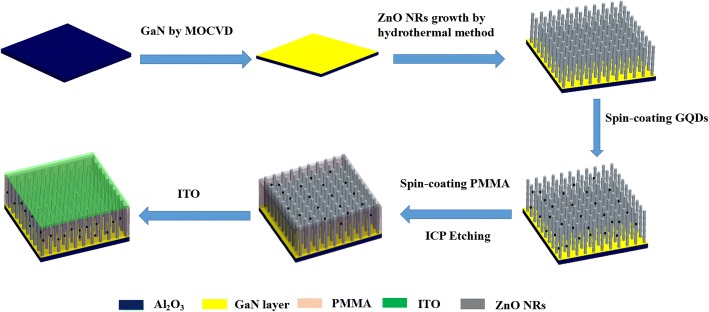
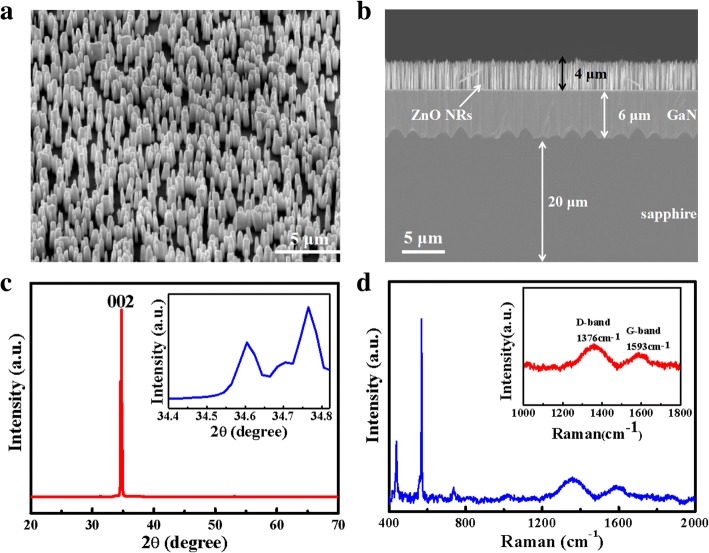
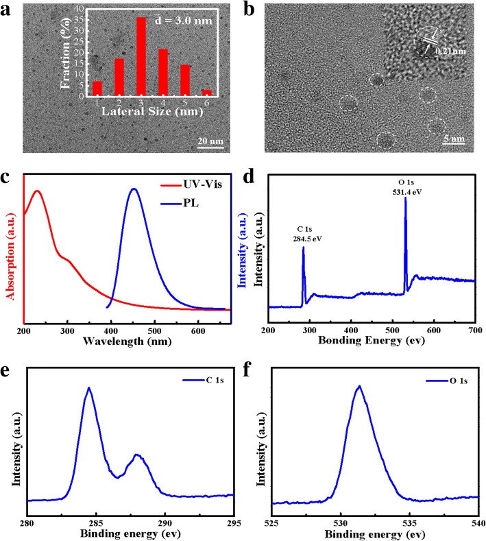
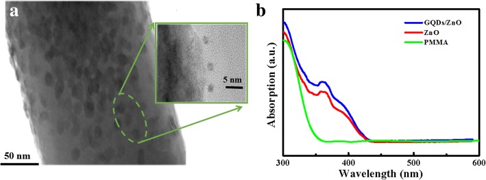
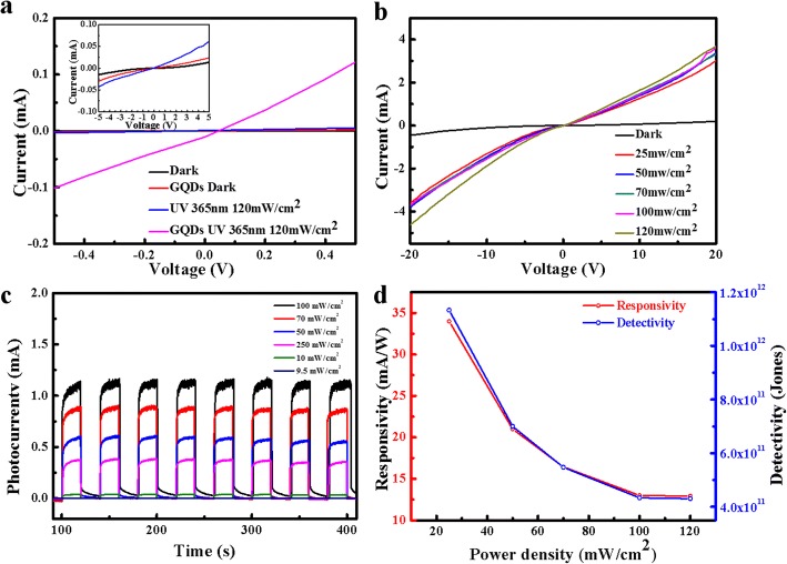
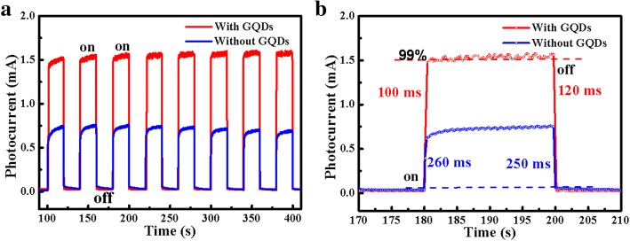
A novel isotype heterojunction ultraviolet photodetector was fabricated by growing n-ZnO nanorod arrays on n-GaN thin films and then spin-coated with graphene quantum dots (GQDs). Exposed to UV illumination with a wavelength of 365 nm, the time-dependent photoresponse of the hybrid detectors manifests high sensitivity and consistent transients with a rise time of 100 ms and a decay time of 120 ms. Meanwhile, an ultra-high specific detectivity (up to ~ 1012 Jones) and high photoresponsivity (up to 34 mA W-1) are obtained at 10 V bias. Compared to the bare heterojunction detectors, the excellent performance of the GQDs decorated n-ZnO/n-GaN heterostructure is attributed to the efficient immobilization of GQDs on the ZnO nanorod arrays. GQDs were exploited as a light absorber and act like an electron donor to effectively improve the effective carrier concentration in interfacial junction. Moreover, appropriate energy band alignment in GQDs decorated ZnO/GaN hybrids can also be a potential factor in facilitating the UV-induced photocurrent and response speed.
Keywords: Graphene quantum dots; Heterojunction; UV photodetector; ZnO nanorod arrays.
Conflict of interest statement
Competing Interests
The authors declare that they have no competing interests.
Publisher’s Note
Springer Nature remains neutral with regard to jurisdictional claims in published maps and institutional affiliations.
Figures

Similar articles
-
Graphene Quantum Dot-Sensitized ZnO-Nanorod/GaN-Nanotower Heterostructure-Based High-Performance UV Photodetectors.ACS Appl Mater Interfaces. 2020 Oct 14;12(41):47038-47047. doi: 10.1021/acsami.0c14246. Epub 2020 Oct 1. ACS Appl Mater Interfaces. 2020. PMID: 32957784
-
Phenomenal Ultraviolet Photoresponsivity and Detectivity of Graphene Dots Immobilized on Zinc Oxide Nanorods.ACS Appl Mater Interfaces. 2016 Dec 28;8(51):35496-35504. doi: 10.1021/acsami.6b13037. Epub 2016 Dec 14. ACS Appl Mater Interfaces. 2016. PMID: 27966848
-
Graphene Quantum Dot-Sensitized ZnO Nanorod/Polymer Schottky Junction UV Detector with Superior External Quantum Efficiency, Detectivity, and Responsivity.ACS Appl Mater Interfaces. 2016 Nov 23;8(46):31822-31831. doi: 10.1021/acsami.6b09766. Epub 2016 Nov 9. ACS Appl Mater Interfaces. 2016. PMID: 27800675
-
Size-Controlled Graphene Nanodot Arrays/ZnO Hybrids for High-Performance UV Photodetectors.Adv Sci (Weinh). 2017 Nov 17;5(1):1700334. doi: 10.1002/advs.201700334. eCollection 2018 Jan. Adv Sci (Weinh). 2017. PMID: 29375965 Free PMC article. Review.
-
Recent advances in development of nanostructured photodetectors from ultraviolet to infrared region: A review.Chemosphere. 2021 Sep;279:130473. doi: 10.1016/j.chemosphere.2021.130473. Epub 2021 Apr 12. Chemosphere. 2021. PMID: 33892456 Review.
Cited by
-
Design and TCAD analysis of few-layer graphene/ZnO nanowires heterojunction-based photodetector in UV spectral region.Sci Rep. 2025 Mar 5;15(1):7762. doi: 10.1038/s41598-025-92596-3. Sci Rep. 2025. PMID: 40044795 Free PMC article.
-
Highly Sensitive, Ultrafast, and Broadband Photo-Detecting Field-Effect Transistor with Transition-Metal Dichalcogenide van der Waals Heterostructures of MoTe2 and PdSe2.Adv Sci (Weinh). 2021 Jun;8(11):e2003713. doi: 10.1002/advs.202003713. Epub 2021 Mar 16. Adv Sci (Weinh). 2021. PMID: 34105276 Free PMC article.
-
Micropreparative Gel Electrophoresis for Purification of Nanoscale Bioconjugates.Bioconjug Chem. 2024 Feb 21;35(2):154-163. doi: 10.1021/acs.bioconjchem.3c00388. Epub 2024 Feb 6. Bioconjug Chem. 2024. PMID: 38320084 Free PMC article.
-
Liquid-Exfoliated 2D Materials for Optoelectronic Applications.Adv Sci (Weinh). 2021 Jun;8(11):e2003864. doi: 10.1002/advs.202003864. Epub 2021 Mar 11. Adv Sci (Weinh). 2021. PMID: 34105282 Free PMC article. Review.
-
Photoluminescence research of the graphene quantum dots (GQD) interaction on the zinc oxide (ZnO) surface for application as H2O2 photosensor.Heliyon. 2024 May 23;10(11):e31144. doi: 10.1016/j.heliyon.2024.e31144. eCollection 2024 Jun 15. Heliyon. 2024. PMID: 39668972 Free PMC article.
References
-
- Gundimeda A, Krishna S, Aggarwal N, et al. Fabrication of non-polar GaN based highly responsive and fast UV photodetector. Appl Phys Lett. 2017;110(10):103507. doi: 10.1063/1.4978427. - DOI
-
- Baghchesara MA, Yousefi R. Photocurrent application of Zn-doped CdS nanostructures grown by thermal evaporation method. Ceram Int. 2016;42(1:1891–1896. doi: 10.1016/j.ceramint.2015.09.158. - DOI
-
- Panda S, Jacob C. Preparation of transparent ZnO thin films and their application in UV sensor devices. Solid State Electron. 2012;73:44–50. doi: 10.1016/j.sse.2012.03.004. - DOI
-
- Przez’dziecka E Stachowicz M Chusnutdinow S et al. Electron beam induced current profiling of the p-ZnO:N/n-GaN heterojunction. Appl Phys Lett. 2015;106(6):062106. doi: 10.1063/1.4908291. - DOI
Grants and funding
LinkOut - more resources
Full Text Sources
Other Literature Sources
