Review
. 2018 Aug 29;19(1):613-648.
doi: 10.1080/14686996.2018.1494493. eCollection 2018.

Structure of graphene and its disorders: a review

Affiliations
Review

Structure of graphene and its disorders: a review

Gao Yang et al. Sci Technol Adv Mater. .

Abstract

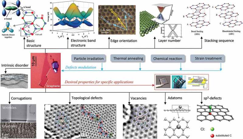
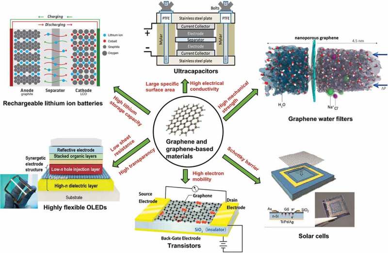
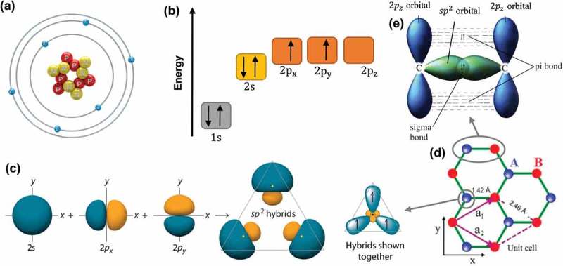
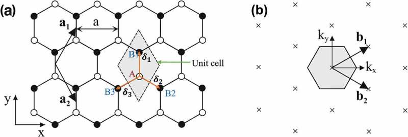
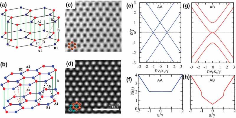
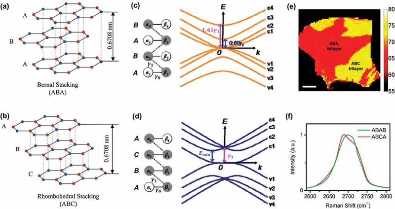
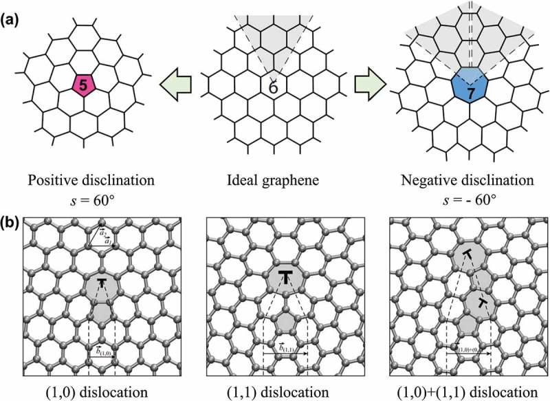
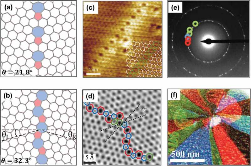
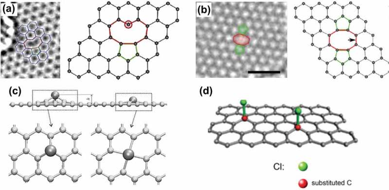
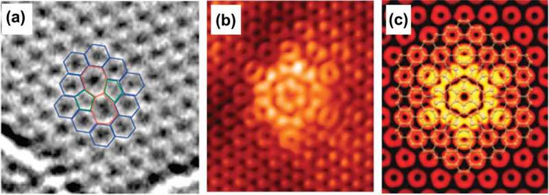
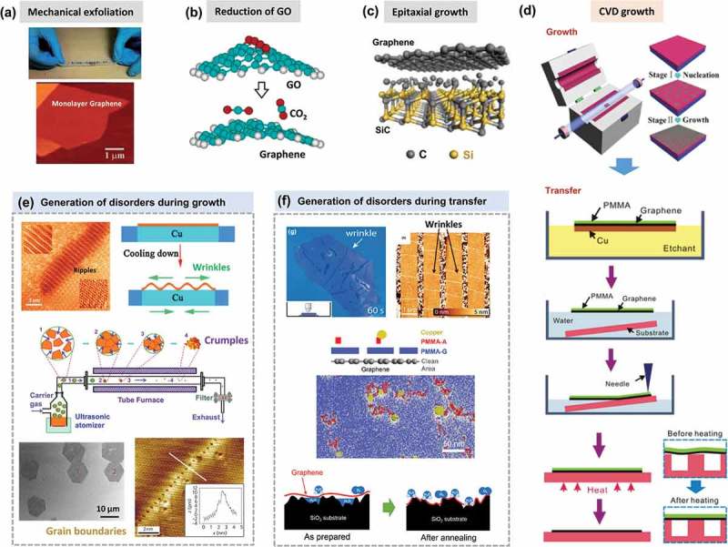
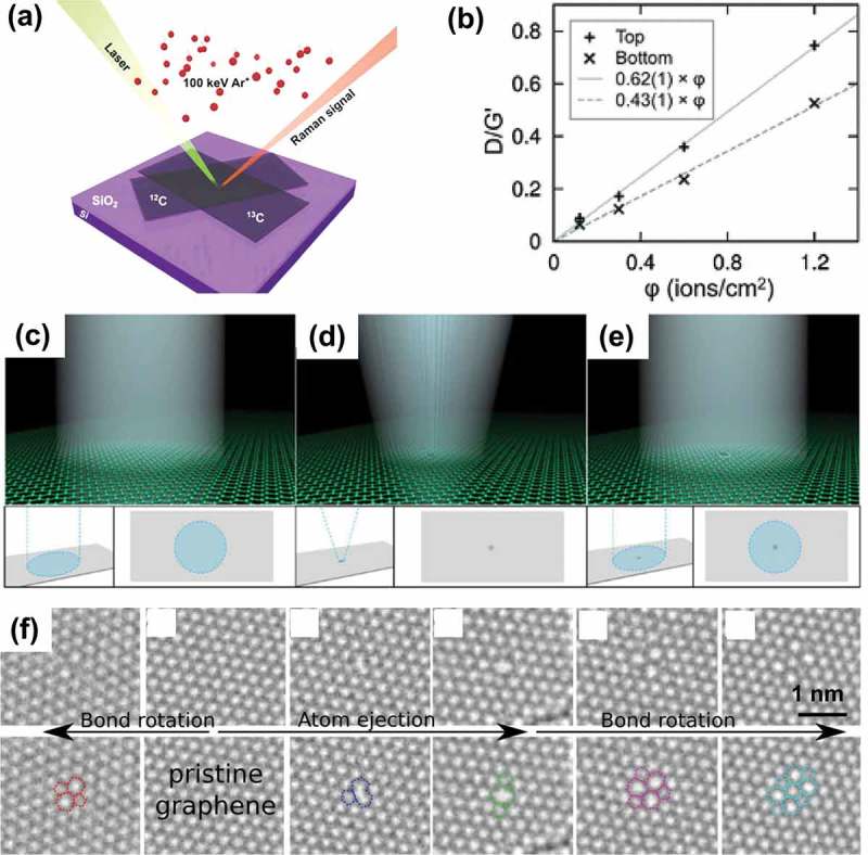
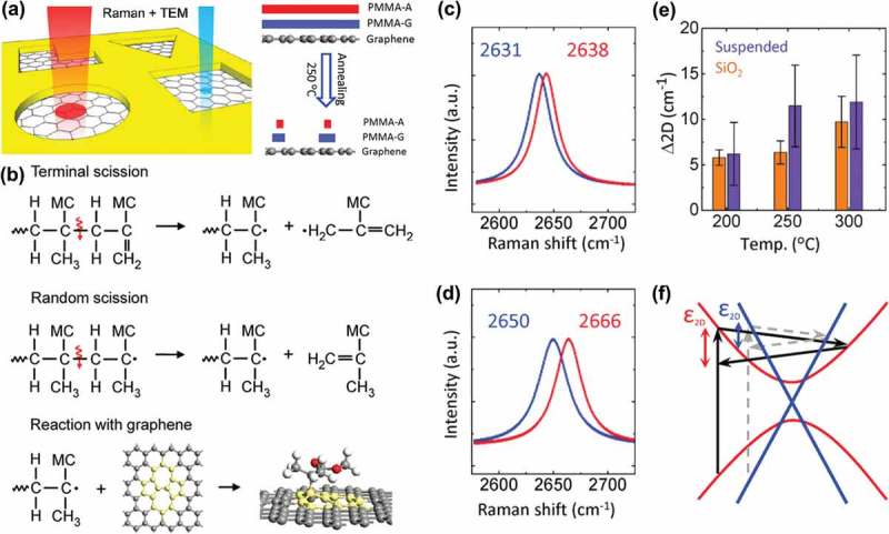
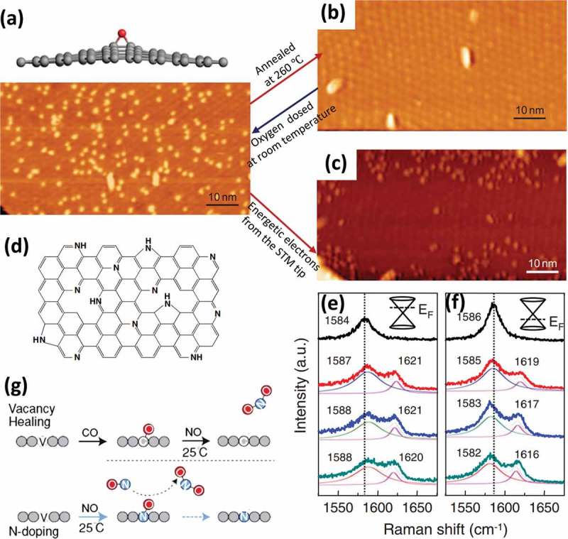
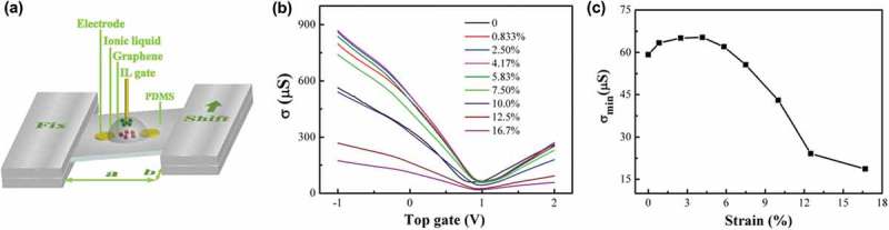
Monolayer graphene exhibits extraordinary properties owing to the unique, regular arrangement of atoms in it. However, graphene is usually modified for specific applications, which introduces disorder. This article presents details of graphene structure, including sp2 hybridization, critical parameters of the unit cell, formation of σ and π bonds, electronic band structure, edge orientations, and the number and stacking order of graphene layers. We also discuss topics related to the creation and configuration of disorders in graphene, such as corrugations, topological defects, vacancies, adatoms and sp3-defects. The effects of these disorders on the electrical, thermal, chemical and mechanical properties of graphene are analyzed subsequently. Finally, we review previous work on the modulation of structural defects in graphene for specific applications.

Keywords: 10 Engineering and Structural materials; 104 Carbon and related materials; 105 Low-Dimension (1D/2D) materials; 2D materials; 302 Crystallization / Heat treatment / Crystal growth; Graphene; defects modulation; disorder; review; structure.


Figures

None
Graphical abstract
Figure 1.
Figure 1.
Applications of graphene and graphene-based materials in batteries, ultracapacitors [20], water filters [43], solar cells [44], transistors and OLEDs [26] (reused with permissions from [20] Copyright © 2008, American Chemical Society, [43] Copyright © 2012, American Chemical Society, and [44] Copyright © 2010, John Wiley and Sons.).
Figure 2.
Figure 2.
(a) Atomic structure of a carbon atom. (b) Energy levels of outer electrons in carbon atoms. (c) The formation of sp2 hybrids. (d) The crystal lattice of graphene, where A and B are carbon atoms belonging to different sub-lattices, a1 and a2 are unit-cell vectors. (e) Sigma bond and pi bond formed by sp2 hybridization.
Figure 3.
Figure 3.
(a) Honeycomb lattice of monolayer graphene, where white (black) circles indicate carbon atoms on A (B) sites, and (b) the reciprocal lattice of monolayer graphene, where the shaded hexagon is the corresponding Brillouin zone [51] (reused with permission from [51] Copyright © 2011, Springer-Verlag Berlin Heidelberg.).
Figure 4.
Figure 4.
(a) Band structure of graphene calculated with a tight-binding method with ϵ2p=0 eV, γ0=3.033 eV and s0=0.129 eV. (b) Cross-section through the band structure, where the energy bands are plotted as a function of wave vector component kx along the line ky=0.
Figure 5.
Figure 5.
(a) Scanning electron microscopy (SEM) image of a relatively large graphene crystal, which shows that most of the crystal’s faces are zigzag and armchair edges, as indicated by blue and red lines and illustrated in the inset [7]. (b) A typical graphene flake obtained by micromechanical cleavage [72]. (c) Sketch of the honeycomb crystal lattice of graphene. Two distinct crystallographic orientations of a graphene crystal, rotated against each other in multiples of 30°, are indicated as armchair type (solid lines) and zigzag type (dashed lines) [72]. (d) CC-STM image of edges of graphene on Ir(111), with crystallographic directions of the Ir substrate denoted at the top-right side [89]. (e) STM image of graphene structures on Co substrate, and schematic of triangular and hexagonal corners, respectively, for zigzag-edged graphene structures on Co(0001) [90]. (f) 20 × 20 nm2 STM image and (g) 2.5 × 2.5 nm2 rendered STM topography of graphene island on 6H-SiC(0001) substrate. Overlaid on this image are the two lowest energy edge directions: zigzag (yellow arrow) and armchair (blue arrows) [75] (reused with permissions from [7] Copyright © 2007, Springer Nature, [72] Rights managed by AIP Publishing, [89] Copyright © 2012 American Physical Society,  [90] Copyright © 2014, American Chemical Society, and [75] Copyright ©2010 American Physical Society.).
Figure 6.
Figure 6.
(a) SEM image of an annealed Cu foil taken out of the furnace after graphene growth [78]. (b) Intensity map of D band for two coalesced graphene grains [78]. (c) A montage of bright field TEM images (80 kV) spliced together to show an example of a hexagonally shaped graphene grain, with its characteristic SAED pattern in the inset [78]. (d) STM topography image taken near a corner of a graphene grain on Cu [78]. (e) Atomic-resolution STM image taken from the area which is marked by a black square in Figure 6(d). (Z: zigzag; A: armchair) [78]. (f) A modified HRTEM image of overlapping zigzag-armchair edges; the HRTEM image is originally from Ref [79], and the modified version is from Ref [111] (reused with permissions from [78] Copyright © 2011, Springer Nature, [79] Copyright © 2009, American Association for the Advancement of Science, and [111] Copyright © 2010 Elsevier Ltd.).
Figure 7.
Figure 7.
Low energy DFT 3D band structure and its projection on kx component close to K point for (a) monolayer graphene, (b) AB-stacked bilayer graphene, (c) ABA-stacked trilayer graphene and (d) bulk graphite. The Fermi level has been set at zero in all cases [111] (reused with permission from [111] Copyright © 2010 Elsevier Ltd.).
Figure 8.
Figure 8.
Evolution of the (a) 514 nm and (b) 633 nm Raman spectra near the 2D peak with the number of graphene layers [140] (reused with permission from [140] Copyright © 2006 American Physical Society.).
Figure 9.
Figure 9.
Stacking arrangements and hopping parameters for (a) AA-stacked and (b) AB-stacked bilayer graphene [166]. Hopping integrals t and t’ correspond to the in-plane nearest-neighboring and next-nearest-neighboring hopping respectively, and parameter t0 is associated with the main interlayer hopping in bilayer. Atomic-resolution STEM images of (c) AA- and (d) AB-stacked bilayer graphenes [156]. Hexagonal ring in the first (second) or bottom (top) layer is marked with green (orange) color. (e) Low energy dispersion and (f) low energy DOS for a bilayer graphene with AA stacking. (g) Low-energy dispersion and (h) low-energy DOS for a bilayer graphene with AB stacking [157] (reused with permissions from [166] © 2016 Elsevier B.V., and [157] Copyright © 2012 American Physical Society.).
Figure 10.
Figure 10.
(a) Bernal and (b) rhombohedral stacking arrangements in multilayer graphene. Electronic band structures of (c) Bernal-stacked and (d) rhombohedral stacked tetralayer graphenes [150]. (e)Raman imaging of the distribution of ABA and ABC trilayer graphene domains [174]. (f) Raman 2D-mode spectra for the tetralayer graphene samples of ABAB (green line) and ABCA (red line) stacking orders [174](reused with permissions from [150] Copyright © 2010 American Physical Society, and [174] Copyright © 2011, American Chemical Society.).
Figure 11.
Figure 11.
A summary illustration of three types of corrugations (i.e. ripples, wrinkles and crumples) [192]. (reused with permission from [192] © 2015 The Authors. Published by Elsevier Ltd.).
Figure 12.
Figure 12.
Configurations of (a) disclinations and (b) dislocations in graphene lattice [207] (reused with permission from [207] Copyright ©2010 American Physical Society.).
Figure 13.
Figure 13.
Configurations of (a) the θ = 21.8° and (b) the θ = 32.2° symmetric large-angle GBs, respectively [137]. (c) STM image of a regular line defect in graphene on the Ni(111) [208]. (d) Aberration-corrected annular ADF-STEM image of two grains which intersect with a relative rotation of 27°, and are stitched together by an aperiodic line of dislocations [209]. (e) Electron diffraction pattern obtained by DF-TEM imaging graphene grains one by one with few-nanometer resolution using an objective aperture filter in the back focal plane through a small range of angles, and repeating this process using several different aperture filters. (f) False-color, DF image overlay of the sizes, shapes and orientations of several grains [209] (reused with permissions from [137] Copyright © 2014, Springer Nature, [208] Copyright © 2010, Springer Nature, and [209] Copyright © 2011, Springer Nature.).
Figure 14.
Figure 14.
Configurations of (a) SV (5–9) [214], (b) double vacancy [214], (c) transition metal atoms adsorbed on single and double vacancies in a graphene sheet [216] and (d) sp3 defects [225] (reused with permissions from [214] Copyright © 2008, American Chemical Society, [50] Copyright © 2011, American Chemical Society, [216] Copyright ©2009 American Physical Society, and [225] © 2017 Elsevier Inc. All rights reserved.).
Figure 15.
Figure 15.
(a) TEM image of a SW defect, formed by rotating a carbon–carbon bond by 90° [214]. (b) STM topography of a sixfold defect observed in the growth of epitaxial graphene on SiC at −300 mV sample bias [228]. (c) Simulated STM image of the C6(1,1) defect using DFT calculations [228] (reused with permissions from [214] Copyright © 2008, American Chemical Society, and [228] Copyright © 2011 American Physical Society.).
Figure 16.
Figure 16.
Fabrication of monolayer graphene by (a) mechanical exfoliation [320], (b) reduction of GO [353], (c) epitaxial growth [354] and (d) CVD growth [321,312]. Generation of disorders during (e) growth [240,192,78,208] and (f) transfer [319,329,322]. In (f), PMMA-A and PMMA-G correspond to PMMA facing the air and graphene respectively. (reused with permissions from [320] Copyright © 2015, Royal Society of Chemistry, [353] Copyright © 2006, American Chemical Society, [354] Copyright © 2013, Tsinghua University Press and Springer-Verlag Berlin Heidelberg, [321] Copyright © 2015, Elsevier. [312] Copyright © 2011, American Chemical Society, [240] Copyright © 2012, Springer Nature, [192] © 2015 The Authors. Published by Elsevier Ltd, [78] Copyright © 2011, Springer Nature, [208] Copyright © 2010, Springer Nature, [319] Rights managed by AIP Publishing, [329] Copyright © 2012, American Chemical Society, and [322] © 2017 Elsevier Ltd. All rights reserved.)
Figure 17.
Figure 17.
(a) Schematic illustration of the experimental setup for the irradiation of Ar+ ions with various doses followed by Raman probing [326]. (b) D/G’ intensity ratios as functions of Ar+ ion irradiation fluence (in 1013 ions/cm2) [326]. Schematics of the beam profile used in the three principle stages [328]: (c) a broad beam used to image graphene before defect formation, (d) a focused beam with a high current density used to form defects and (e) a broad beam used to image graphene after defect formation. (f) Creation of the defects can be explained by atom ejection and reorganization of bonds via bondrotation [339] (reused with permissions from [326] Copyright © 2012, John Wiley and Sons, [328] Copyright © 2012, Springer Nature, and [339] Copyright © 2011 American Physical Society).
Figure 18.
Figure 18.
(a) Schematic illustration of a combination of TEM observation and Raman spectroscopy for graphene. PMMA-A and PMMA-G correspond to PMMA facing the air and graphene respectively. Comparisons of the 2D peak positions before and after annealing for (c) Si-supported and (d) free-standing CVD graphenes. (e) Histogram of the Δ2D as a function of annealing temperature for both Si-supported and free-standing graphenes. (f) Schematic illustration of the electronic structure near the Dirac points of pristine (linear) and annealed (parabolic) CVD graphenes. All pictures are extracted from Ref [329] (reused with permission from [329] Copyright © 2012, American Chemical Society.).
Figure 19.
Figure 19.
(a) Configuration of chemisorbed oxygen on graphene sheet, which corresponds to bright protrusions in bottom Auger electron spectroscopy (AES) image [345]. STM images of UHV oxidized epitaxial graphene after (b) annealing at 260 °C and (c) reversibly desorbed by injecting electrons from the STM tip at a sample bias of + 4V and tunneling current of 1 nA [345]. (d) Schematic of postulated nitrogenation on graphene [346]. The evolution of G peak upon plasma exposure for graphene with initial Fermi level lying in (e) conduction band and (f) valance band, respectively. The dashed lines indicate the G peak position of pristine graphene [346]. (g) Schematic view of the vacancy healing and N-doping processes of graphene by chemical reactions [331] (reused with permissions from [345] Copyright © 2012, Springer Nature, [346], Rights managed by AIP Publishing, and [331] Copyright ©2011 American Physical Society.).
Figure 20.
Figure 20.
(a) Schematic of the strain device: The red balls represent negative ions, and the green balls represent positive ions of ionic liquid (IL). PDMS stands for polydimethylsiloxane. (b) Transfer characteristics of the ionic liquid gated graphene under different strains. (c) Conductance of the Dirac points under different strains [334] (reused with permission from [334] Rights managed by AIP Publishing.).

References

    1. Wallace PR. The band theory of graphite. Phys Rev. 1947;71:622–634.
    1. Fradkin E. Critical behavior of disordered degenerate semiconductors. II. Spectrum and transport properties in mean-field theory. Phys Rev B. 1986;33:3263–3268. - PubMed
    1. Mermin ND. Crystalline order in two dimensions. Phys Rev. 1968;176:250–254.
    1. Land TA, Michely T, Behm RJ, et al. STM investigation of single layer graphite structures produced on Pt(111) by hydrocarbon decomposition. Surf Sci. 1992;264:261–270.
    1. Ohashi Y, Koizumi T, Yoshikawa T, et al. Size effect in the in-plane electrical resistivity of very thin graphite crystals. Tanso. 1997;1997:235–238.

LinkOut - more resources