Conductively coupled flexible silicon electronic systems for chronic neural electrophysiology
- PMID: 30228119
- PMCID: PMC6187144
- DOI: 10.1073/pnas.1813187115
Conductively coupled flexible silicon electronic systems for chronic neural electrophysiology
Abstract
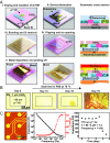
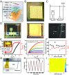
Materials and structures that enable long-term, intimate coupling of flexible electronic devices to biological systems are critically important to the development of advanced biomedical implants for biological research and for clinical medicine. By comparison with simple interfaces based on arrays of passive electrodes, the active electronics in such systems provide powerful and sometimes essential levels of functionality; they also demand long-lived, perfect biofluid barriers to prevent corrosive degradation of the active materials and electrical damage to the adjacent tissues. Recent reports describe strategies that enable relevant capabilities in flexible electronic systems, but only for capacitively coupled interfaces. Here, we introduce schemes that exploit patterns of highly doped silicon nanomembranes chemically bonded to thin, thermally grown layers of SiO2 as leakage-free, chronically stable, conductively coupled interfaces. The results can naturally support high-performance, flexible silicon electronic systems capable of amplified sensing and active matrix multiplexing in biopotential recording and in stimulation via Faradaic charge injection. Systematic in vitro studies highlight key considerations in the materials science and the electrical designs for high-fidelity, chronic operation. The results provide a versatile route to biointegrated forms of flexible electronics that can incorporate the most advanced silicon device technologies with broad applications in electrical interfaces to the brain and to other organ systems.
Keywords: bioelectronics; brain interface; flexible electronics; neuroscience.
Conflict of interest statement
The authors declare no conflict of interest.
Figures


Similar articles
-
Ultrathin, Transferred Layers of Metal Silicide as Faradaic Electrical Interfaces and Biofluid Barriers for Flexible Bioelectronic Implants.ACS Nano. 2019 Jan 22;13(1):660-670. doi: 10.1021/acsnano.8b07806. Epub 2019 Jan 10. ACS Nano. 2019. PMID: 30608642
-
Ultrathin, transferred layers of thermally grown silicon dioxide as biofluid barriers for biointegrated flexible electronic systems.Proc Natl Acad Sci U S A. 2016 Oct 18;113(42):11682-11687. doi: 10.1073/pnas.1605269113. Proc Natl Acad Sci U S A. 2016. PMID: 27791052 Free PMC article.
-
Long-Lived, Transferred Crystalline Silicon Carbide Nanomembranes for Implantable Flexible Electronics.ACS Nano. 2019 Oct 22;13(10):11572-11581. doi: 10.1021/acsnano.9b05168. Epub 2019 Aug 26. ACS Nano. 2019. PMID: 31433939
-
Materials for flexible bioelectronic systems as chronic neural interfaces.Nat Mater. 2020 Jun;19(6):590-603. doi: 10.1038/s41563-020-0679-7. Epub 2020 May 27. Nat Mater. 2020. PMID: 32461684 Review.
-
How is flexible electronics advancing neuroscience research?Biomaterials. 2021 Jan;268:120559. doi: 10.1016/j.biomaterials.2020.120559. Epub 2020 Dec 2. Biomaterials. 2021. PMID: 33310538 Free PMC article. Review.
Cited by
-
Neurosurgery and the Brain-Computer Interface.Adv Exp Med Biol. 2024;1462:513-527. doi: 10.1007/978-3-031-64892-2_32. Adv Exp Med Biol. 2024. PMID: 39523287 Review.
-
Soft-Hard Composites for Bioelectric Interfaces.Trends Chem. 2020 Jun;2(6):519-534. doi: 10.1016/j.trechm.2020.03.005. Epub 2020 Apr 23. Trends Chem. 2020. PMID: 34296076 Free PMC article.
-
Ultra-Thin Flexible Encapsulating Materials for Soft Bio-Integrated Electronics.Adv Sci (Weinh). 2022 Oct;9(30):e2202980. doi: 10.1002/advs.202202980. Epub 2022 Aug 28. Adv Sci (Weinh). 2022. PMID: 36031395 Free PMC article. Review.
-
Recent advances in bioelectronics chemistry.Chem Soc Rev. 2020 Nov 21;49(22):7978-8035. doi: 10.1039/d0cs00333f. Epub 2020 Jul 16. Chem Soc Rev. 2020. PMID: 32672777 Free PMC article. Review.
-
Electronic and Thermal Properties of Graphene and Recent Advances in Graphene Based Electronics Applications.Nanomaterials (Basel). 2019 Mar 5;9(3):374. doi: 10.3390/nano9030374. Nanomaterials (Basel). 2019. PMID: 30841599 Free PMC article. Review.
References
-
- McKhann GM, 2nd, Schoenfeld-McNeill J, Born DE, Haglund MM, Ojemann GA. Intraoperative hippocampal electrocorticography to predict the extent of hippocampal resection in temporal lobe epilepsy surgery. J Neurosurg. 2000;93:44–52. - PubMed
Publication types
MeSH terms
Substances
LinkOut - more resources
Full Text Sources
Other Literature Sources

