. 2018 Jun 5;5(9):1800346.
doi: 10.1002/advs.201800346. eCollection 2018 Sep.

3D Nanofabrication of High-Resolution Multilayer Fresnel Zone Plates

Affiliations

3D Nanofabrication of High-Resolution Multilayer Fresnel Zone Plates

Umut Tunca Sanli et al. Adv Sci (Weinh). .

Abstract

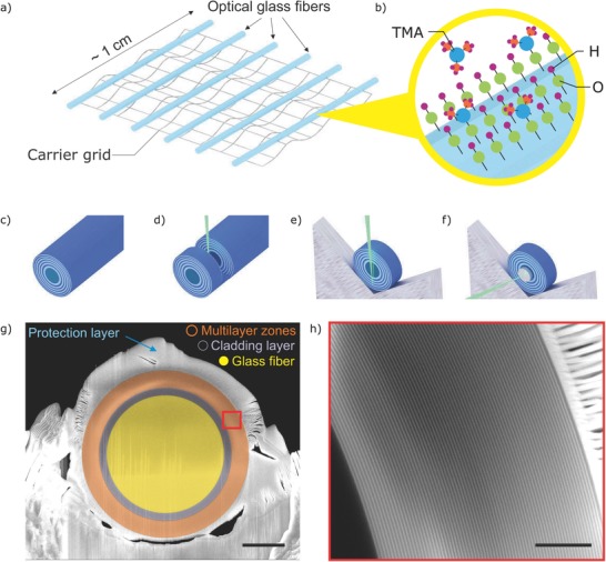
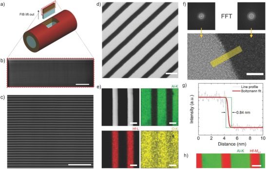
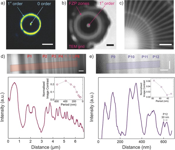
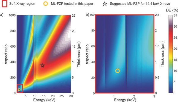
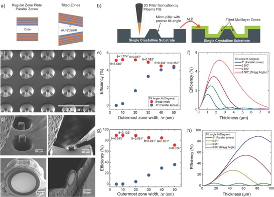
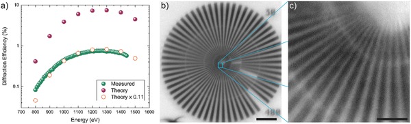
Focusing X-rays to single nanometer dimensions is impeded by the lack of high-quality, high-resolution optics. Challenges in fabricating high aspect ratio 3D nanostructures limit the quality and the resolution. Multilayer zone plates target this challenge by offering virtually unlimited and freely selectable aspect ratios. Here, a full-ceramic zone plate is fabricated via atomic layer deposition of multilayers over optical quality glass fibers and subsequent focused ion beam slicing. The quality of the multilayers is confirmed up to an aspect ratio of 500 with zones as thin as 25 nm. Focusing performance of the fabricated zone plate is tested toward the high-energy limit of a soft X-ray scanning transmission microscope, achieving a 15 nm half-pitch cut-off resolution. Sources of adverse influences are identified, and effective routes for improving the zone plate performance are elaborated, paving a clear path toward using multilayer zone plates in high-energy X-ray microscopy. Finally, a new fabrication concept is introduced for making zone plates with precisely tilted zones, targeting even higher resolutions.

Keywords: X‐ray optics; atomic layer deposition; focused ion beam; fresnel zone plates; nanofabrication.


Figures

Figure 1
Figure 1
Fabrication stages of ML‐FZP. a) Numerous glass fibers are mounted on a grid. b) Multilayer zones are deposited via ALD. Here, the deposition of the first Al2O3 layer is depicted by a pulse of trimethylaluminum (TMA) on an OH activated surface. A long deposited fiber c) is sliced d) and mounted on a Mo lift‐out grid e) in the dual beam instrument. f) A beam stopping Pt layer is deposited via ion beam induced deposition in the FIB. g) Scanning electron microscopy (SEM) image of the ML‐FZP mounted on a Mo lift‐out grid. Scale bar is 10 µm. h) SEM image of the multilayer zones defined with the red square of (g). Scale bar is 1 µm.
Figure 2
Figure 2
Characterization of multilayer zones along the optical axis. a) Illustration showing location and orientation of the imaged sample. A rectangular prism is lifted out from the deposited fiber by using FIB. b) HAADF image of the lifted out lamella captured using STEM mode in dual beam instrument. The aspect ratio of the structure is larger than 500. Scale bar is 2 µm. c) Higher magnification image of the same lamella shows linear high‐aspect‐ratio multilayer zones. Scale bar is 500 nm. d) STEM bright‐field image of the zones. Scale bar is 50 nm. e) STEM HAADF image and EDX maps of Al–K, Hf–L, and O–K. Scale bars are identical and correspond to 25 nm. f) HRTEM image of the Al2O3–HfO2 interface and FFT confirming fully amorphous zones. Scale bar is 5 nm. g) Intensity line profile of the yellow region of the HRTEM image confirming molecularly sharp interface well below 1 nm. FWHM of the first derivative to the fitted curve is 0.33 nm. h) STEM EELS map of Al–K and Hf–M4, 5. Multiple linear least square fitting was used to subtract the background. Scale bar is 20 nm.
Figure 3
Figure 3
Synchrotron experiments at BESSY II, UE46‐PGM2. a) Charge coupled device (CCD) image of a scintillator screen showing the 1st order diffraction ring. For this image an order selecting aperture was placed between the FZP and CCD. The scintillator screen was placed further away from the focal point and the image on screen was magnified onto the CCD detector. The ML‐FZP tilt was corrected via a tilt stage until a circular first order focus ring was obtained. The presence of the zero order hints a misalignment of the OSA. The scale bar is 250 nm−1. b) Pinhole scan over the FZP to measure the diffraction efficiency. The transmitted light is collected by an avalanche photo diode (APD). Dwell time 2 ms. Step size 500 nm × 500 nm. Photon energy 1400 eV. Scale bar is 10 µm. c) STXM image of the Siemens Star test pattern. The 30 nm features of the innermost ring are resolved. Dwell time 10 ms. Energy 1198 eV. Step size 10 × 10 nm. Scale bar is 500 nm. d) STXM image of P1 to P8 of the BAM L‐200 test structure (top) and its integrated intensity profile and normalized Michelson image contrast (bottom graph). All features P1 (587 nm)–P8 (48.5 nm) are resolved. Dwell time 10 ms. Step size 10 × 10 nm. Photon energy 1200 eV. Scale bar is 500 nm. e) STXM image of the P9 (76.5 nm) to P12 (30 nm) of the BAM L‐200 test structure (top) and its integrated (15 pixels wide) intensity profile and normalized Michelson image contrast (bottom graph). 30 nm full period structure (P12) is resolved corresponding to 15 nm half‐pitch cut‐off resolution. Dwell time 30 ms. Step size 4 × 5 nm. Photon energy is 1296 eV. Scale bars correspond to horizontal 100 nm and vertical 120 nm.
Figure 4
Figure 4
Diffraction efficiency maps of Al2O3–HfO2 ML‐FZP. Calculations were done according to thin grating approximation as a function of aspect ratio, optical thickness and X‐ray energy for Δr = 25 nm. a) Diffraction efficiency map from 100 eV to 30 keV. b) Diffraction efficiency map of the region marked in red in (a). The corresponding numbers to color coding represents the diffraction efficiency in percent.
Figure 5
Figure 5
a) In tilted ML‐FZP the zones are tilted with respect to the optical axis. The peak efficiency is achieved if the zones are tilted to the Bragg angle. The concept of regular ML‐FZP with parallel zones and the suggested ML‐FZP with tilted zones is sketched in a side view. b) The fabrication steps of tilted ML‐FZPs is illustrated. c) An SEM image of the tapered micropillar array fabricated via Plasma Focused Ion Beam (PFIB). Multilayer zones of Al2O3–SiO2 are deposited on the tilted micropillar array using ALD. d) A planar liftout strategy is followed to prepare tilted ML‐FZPs from the deposited array. Individual tilted ML‐FZPs are then mounted on Mo lift‐out grids similar to regular ML‐FZPs. e) Calculated diffraction efficiencies of ML‐FZPs at their optimum optical thickness having parallel and tilted zones as a function of outermost zone width, Δr for 1 keV X‐rays. f) Calculated diffraction efficiency of an Al2O3–SiO2 ML‐FZP of Δr = 20 nm for 1 keV X‐rays as a function of tilt angle, θ. g) Calculated diffraction efficiencies of ML‐FZPs at their optimum optical thickness having parallel and tilted zones as a function of outermost zone width, Δr for 14.4 keV X‐rays. h) Calculated diffraction efficiency of an Al2O3–SiO2 ML‐FZP of Δr = 20 nm for 14.4 keV X‐rays as a function of tilt angle, θ. All the efficiencies are calculated according to CWT locally, considering only the outermost period and not integrated to the FZP area.
Figure 6
Figure 6
a) Measured (green spheres) versus theoretical diffraction efficiencies (purple spheres and orange circles) for the tilted ML‐FZPs. The theoretical calculations were done according to CWT. The difference of the thickness of each period was taken into account (nonlocal, integrated). b) STXM image of the Siemens Star test sample. Energy is 1175 eV. Step size is 20 nm. Scale bar is 5 µm. c) STXM image of a quarter of the inner rings of the Siemens Star test sample. Energy is 1175 eV. Step size is 10 nm. Scale bar is 500 nm.

References

    1. Chao W., Fischer P., Tyliszczak T., Rekawa S., Anderson E., Naulleau P., Opt. Express 2012, 20, 9777. - PubMed
    1. Vila‐Comamala J., Jefimovs K., Raabe J., Pilvi T., Fink R. H., Senoner M., Maaßdorf A., Ritala M., David C., Ultramicroscopy 2009, 109, 1360. - PubMed
    1. Rehbein S., Guttmann P., Werner S., Schneider G., Opt. Express 2012, 20, 5830. - PubMed
    1. Shapiro D. A., Yu Y.‐S., Tyliszczak T., Cabana J., Celestre R., Chao W., Kaznatcheev K., Kilcoyne A. D., Maia F., Marchesini S., Shirley Meng Y., Warwick T., Yang L. L., Padmore H. A., Nat. Photonics 2014, 8, 765.
    1. Sakdinawat A., Attwood D., Nat. Photonics 2010, 4, 840.