. 2018 Sep 21;4(9):eaau0920.
doi: 10.1126/sciadv.aau0920. eCollection 2018 Sep.

2D titanium carbide (MXene) for wireless communication

Affiliations

2D titanium carbide (MXene) for wireless communication

Asia Sarycheva et al. Sci Adv. .

Abstract

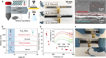
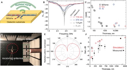
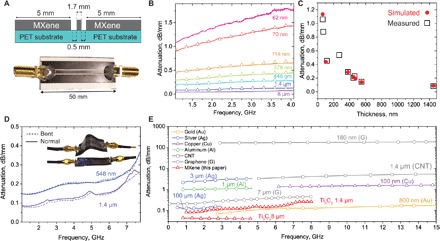
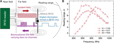
With the development of the Internet of Things (IoT), the demand for thin and wearable electronic devices is growing quickly. The essential part of the IoT is communication between devices, which requires radio-frequency (RF) antennas. Metals are widely used for antennas; however, their bulkiness limits the fabrication of thin, lightweight, and flexible antennas. Recently, nanomaterials such as graphene, carbon nanotubes, and conductive polymers came into play. However, poor conductivity limits their use. We show RF devices for wireless communication based on metallic two-dimensional (2D) titanium carbide (MXene) prepared by a single-step spray coating. We fabricated a ~100-nm-thick translucent MXene antenna with a reflection coefficient of less than -10 dB. By increasing the antenna thickness to 8 μm, we achieved a reflection coefficient of -65 dB. We also fabricated a 1-μm-thick MXene RF identification device tag reaching a reading distance of 8 m at 860 MHz. Our finding shows that 2D titanium carbide MXene operates below the skin depth of copper or other metals as well as offers an opportunity to produce transparent antennas. Being the most conductive, as well as water-dispersible, among solution-processed 2D materials, MXenes open new avenues for manufacturing various classes of RF and other portable, flexible, and wearable electronic devices.


Figures

Fig. 1
Fig. 1. Ti3C2 MXene films and antennas and their processing.
(A) Schematic of multilayered and delaminated forms of 2D Ti3C2 MXene. Top: Atomistic model of a single Ti3C2Tx flake. A single Ti3C2Tx flake has a thickness of ~1 nm. Delaminated single flakes form a stable colloidal solution (MXene ink) and can be processed into freestanding films by vacuum-assisted filtration or sprayed with an air spray gun onto a substrate. (B) Digital photo showing 62-nm-thick (top) and 1.4-μm-thick (bottom) MXene dipole antennas. (C) Cross-sectional scanning electron microscopy (SEM) image of the sprayed MXene (red dashed line). The inset is a top view of the film, where individual Ti3C2 flakes are highlighted with red dotted lines. (D) X-ray diffraction (XRD) patterns of MXene films prepared by vacuum-assisted filtration (black solid line) and after treatment in vacuum at 150°C (red solid line). Thermal treatment of the MXene film shifts the (002) MXene peak position from 6.8° to 8.3°. The same comparison was made with the sprayed 1.4-μm-thick MXene film on PET, as-sprayed MXene film (black dashed line), and the film was heated in vacuum at 150°C (red dashed line). Annealing changed the (002) peak position from ~5° to 6.1° and increased its intensity. The peak around 23° is attributed to the PET substrate. (E) Sheet resistance versus thickness of sprayed MXene films. Inset shows transmittance in the visible range of light for the thinnest antennas. (F) Digital photos of sprayed MXene dipole antennas bent at different curvatures, showing the stability of the deposited layer and its adhesion to the substrate.
Fig. 2
Fig. 2. Ti3C2 MXene antennas and their performance measurements.
(A) Schematic explaining the working principle of the dipole antenna. The length of the dipole antenna matches half of the wavelength of the radiated signal. (B) S11 parameter (reflection coefficient) of dipole antennas of various thicknesses (from 114 nm to 8 μm). Measured values are presented as solid lines, and simulated values are presented as dashed lines. (C) Voltage standing wave ratio (VSWR) of measured MXene antennas, which represents how efficiently power is transmitted to the antenna and impedance matching. Red and blue symbols represent VSWR of copper and aluminum foils, respectively. (D) Digital photo of an experiment in anechoic chamber to measure the radiation pattern of dipole antennas. The Vivaldi antenna was used as the receiving antenna, whereas the radiating antenna was made of MXene. (E) Typical radiation pattern of the 8-μm-thick MXene antenna measured in the anechoic chamber. (F) MXene antennas’ maximum gain versus the antenna thickness. Red circles represent the simulated gain values.
Fig. 3
Fig. 3. MXene TLs and their attenuations.
(A) Schematic and digital photo of the MXene CPW TLs, where MXene was sprayed as a 1.4-μm-thick film. (B) Attenuation of MXene films of various thicknesses (from 62 nm to 8 μm) versus frequency measured using MXene TLs. (C) Attenuation in dB/mm value at 1 GHz versus sheet resistance for various MXene film thicknesses. (D) Attenuation versus frequency of normal (solid line) and bent (dashed line) TLs for MXene film thicknesses of 1.4 μm and 550 nm. No changes could be observed, which shows flexibility of MXene TLs. (E) Comparison of attenuation in CPW of different materials: graphene (12, 29), CNT (30), Ag ink (24), Ag-polydimethylsiloxane (31), Au ink (32), Al (33), and Cu (33) with 1.4- and 8-μm-thick Ti3C2 MXene films.
Fig. 4
Fig. 4. MXene RFID antennas.
(A) General mechanism of RFID working principle. A signal is sent from an RFID reader, received by an RFID antenna connected to an RFID chip. Using the chip, the signal is transformed and backscattered to the reader. (B) MXene RFID antenna (1 μm thick) performance with various characteristic impedances. The impedance can be tuned by tuning the design, particularly the loop. The reading range reaches 8 m when matching the impedance of the chip.

References

    1. Al-Fuqaha A., Guizani M., Mohammadi M., Aledhari M., Ayyash M., Internet of things: A survey on enabling technologies, protocols, and applications. IEEE Commun. Surv. Tutorials 17, 2347–2376 (2015).
    1. D. M. Pozar, Microwave Engineering (John Wiley & Sons, 2009).
    1. Zeng W., Shu L., Li Q., Chen S., Wang F., Tao X. M., Fiber-based wearable electronics: A review of materials, fabrication, devices, and applications. Adv. Mater. 26, 5310–5336 (2014). - PubMed
    1. N. J. Kirsch, N. A. Vacirca, E. E. Plowman, T. P. Kurzweg, A. K. Fontecchio, K. R. Dandekar, Optically transparent conductive polymer RFID meandering dipole antenna, in 2009 IEEE International Conference on RFID, Orlando, FL, 27 to 28 April 2009 (IEEE, 2009), pp. 278–282.
    1. Park M, Im J., Shin M., Min Y., Park J., Cho H., Park S., Shim M.-B, Jeon S., Chang D.-Y., Bae J., Park J., Jeong U., Kim K., Highly stretchable electric circuits from a composite material of silver nanoparticles and elastomeric fibres. Nat. Nanotechnol. 7, 803–809 (2012). - PubMed

Publication types