

Aqueous Synthesis, Degradation, and Encapsulation of Copper Nanowires for Transparent Electrodes
- PMID: 30274162
- PMCID: PMC6215155
- DOI: 10.3390/nano8100767
Aqueous Synthesis, Degradation, and Encapsulation of Copper Nanowires for Transparent Electrodes
Abstract
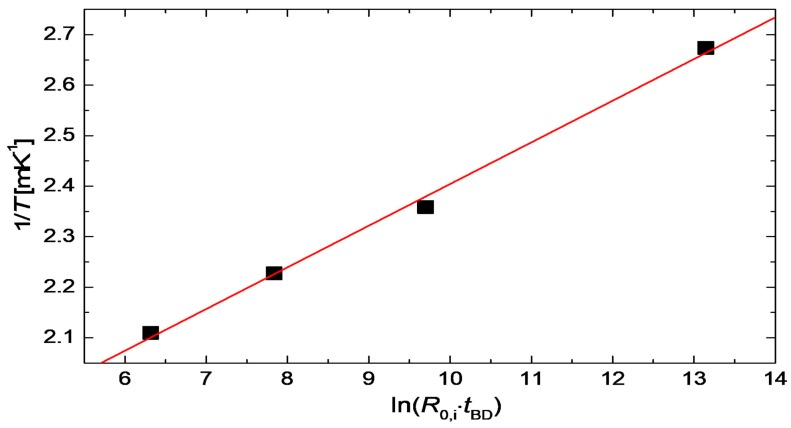
Copper nanowires (CuNWs) have increasingly become subjected to academic and industrial research, which is attributed to their good performance as a transparent electrode (TE) material that competes with the one of indium tin oxide (ITO). Recently, an environmentally friendly and aqueous synthesis of CuNWs was demonstrated, without the use of hydrazine that is known for its unfavorable properties. In this work, we extend the current knowledge for the aqueous synthesis of CuNWs by studying their up-scaling potential. This potential is an important aspect for the commercialization and further development of CuNW-based devices. Due to the scalability and homogeneity of the deposition process, spray coating was selected to produce films with a low sheet resistance of 7.6 Ω/sq. and an optical transmittance of 77%, at a wavelength of 550 nm. Further, we present a comprehensive investigation of the degradation of CuNWs when subjected to different environmental stresses such as the exposure to ambient air, elevated temperatures, high electrical currents, moisture or ultraviolet (UV) light. For the oxidation process, a model is derived to describe the dependence of the breakdown time with the temperature and the initial resistance. Finally, polymer coatings made of polydimethylsiloxane (PDMS) and polymethylmethacrylate (PMMA), as well as oxide coatings composed of electron beam evaporated silicon dioxide (SiO₂) and aluminum oxide (Al₂O₃) are tested to hinder the oxidation of the CuNW films under current flow.
Keywords: CuNWs; PDMS; PMMA; copper nanowires; degradation; encapsulation; solution-based; transparent electrode.
Conflict of interest statement
The authors declare no conflict of interest.
Figures


Similar articles
-
Synchronously improved reliability, figure of merit and adhesion of flexible copper nanowire networks by chitosan transition.Nanotechnology. 2020 Sep 11;31(37):375303. doi: 10.1088/1361-6528/ab967b. Epub 2020 May 26. Nanotechnology. 2020. PMID: 32454475
-
A Green Approach for High Oxidation Resistance, Flexible Transparent Conductive Films Based on Reduced Graphene Oxide and Copper Nanowires.Nanoscale Res Lett. 2022 Aug 24;17(1):79. doi: 10.1186/s11671-022-03716-1. Nanoscale Res Lett. 2022. PMID: 36001189 Free PMC article.
-
Large-Scale Stretchable Semiembedded Copper Nanowire Transparent Conductive Films by an Electrospinning Template.ACS Appl Mater Interfaces. 2017 Aug 9;9(31):26468-26475. doi: 10.1021/acsami.7b08606. Epub 2017 Jul 31. ACS Appl Mater Interfaces. 2017. PMID: 28731322
-
Advancements in Copper Nanowires: Synthesis, Purification, Assemblies, Surface Modification, and Applications.Small. 2018 Jun;14(26):e1800047. doi: 10.1002/smll.201800047. Epub 2018 Apr 30. Small. 2018. PMID: 29707894 Review.
-
Copper Nanowires and Their Applications for Flexible, Transparent Conducting Films: A Review.Nanomaterials (Basel). 2016 Mar 9;6(3):47. doi: 10.3390/nano6030047. Nanomaterials (Basel). 2016. PMID: 28344304 Free PMC article. Review.
Cited by
-
Room Temperature Curable Copper Nanowire-Based Transparent Heater.ACS Omega. 2023 Jun 5;8(23):21107-21112. doi: 10.1021/acsomega.3c02048. eCollection 2023 Jun 13. ACS Omega. 2023. PMID: 37332811 Free PMC article.
-
A Facile and Efficient Protocol for Preparing Residual-Free Single-Walled Carbon Nanotube Films for Stable Sensing Applications.Nanomaterials (Basel). 2019 Mar 21;9(3):471. doi: 10.3390/nano9030471. Nanomaterials (Basel). 2019. PMID: 30901851 Free PMC article.
-
Over-Stretching Tolerant Conductors on Rubber Films by Inkjet-Printing Silver Nanoparticles for Wearables.Polymers (Basel). 2018 Dec 19;10(12):1413. doi: 10.3390/polym10121413. Polymers (Basel). 2018. PMID: 30961338 Free PMC article.
-
Electrical and Thermal Properties of Surface-Modified Copper Nanowire/Polystyrene Nanocomposites through Latex Blending.ACS Omega. 2023 Nov 29;8(49):46955-46966. doi: 10.1021/acsomega.3c06775. eCollection 2023 Dec 12. ACS Omega. 2023. PMID: 38107942 Free PMC article.
-
Rapid Catalytic Reduction of 4-Nitrophenol and Clock Reaction of Methylene Blue using Copper Nanowires.Nanomaterials (Basel). 2019 Jun 28;9(7):936. doi: 10.3390/nano9070936. Nanomaterials (Basel). 2019. PMID: 31261696 Free PMC article.
References
-
- Vosgueritchian M., Lipomi D.J., Bao Z. Highly conductive and transparent PEDOT:PSS films with a fluorosurfactant for stretchable and flexible transparent electrodes. Adv. Funct. Mater. 2012;22:421–428. doi: 10.1002/adfm.201101775. - DOI
-
- Meng L., dos Santos M. Properties of indium tin oxide films prepared by rf reactive magnetron sputtering at different substrate temperature. Thin Solid Films. 1998;322:56–62. doi: 10.1016/S0040-6090(97)00939-5. - DOI
Grants and funding
LinkOut - more resources
Full Text Sources
Other Literature Sources
