. 2018 Dec;12(6):1256-1266.
doi: 10.1109/TBCAS.2018.2876069. Epub 2018 Oct 15.

A 250 μm × 57 μm Microscale Opto-electronically Transduced Electrodes (MOTEs) for Neural Recording

A 250 μm × 57 μm Microscale Opto-electronically Transduced Electrodes (MOTEs) for Neural Recording

Sunwoo Lee et al. IEEE Trans Biomed Circuits Syst. 2018 Dec.

Abstract

Recording neural activity in live animals in vivo with minimal tissue damage is one of the major barriers to understanding the nervous system. This paper presents the technology for a tetherless opto-electronic neural interface based on 180 nm CMOS circuits, heterogeneously integrated with an AlGaAs diode that functions as both a photovoltaic and light emitting diode. These microscale opto-electrically transduced electrodes (MOTEs) are powered by and communicate through an optical interface, simultaneously enabling high temporal-resolution electrical measurements without a tether or a bulky RF coil. The MOTE presented here is 250 μm × 57 μm, consumes 1 μW of electrical power, and is capable of capturing and encoding neural signals before transmitting the encoded signals. The measured noise floor is as low as 15 μVRMS at a 15 kHz bandwidth.


Figures

Fig. 1.
Fig. 1.
Overview of MOTE and its envisioned implementation. Ideally, MOTEs can be implanted into a subject without hindering subject’s freedom of motion. Because a MOTE is optically powered, and transmits the measured neural signals optically as well, the subject needs to be optically accessible, similar to in imaging. In this figure, a mouse on a trackball is shown as an example where the mouse can move almost freely while overhanging optics provide the power as well as signal detection.
Fig. 2.
Fig. 2.
System overview of a MOTE [20]: (a) an exemplary signal flow through the CMOS circuitry followed by the external detector and decoder; (b) a MOTE block diagram in PV mode; (c) a MOTE block diagram in LED mode.
Fig. 3.
Fig. 3.
Simplified schematic of complementary, invertor-based band-passing amplifier employed in MOTE. The amplifier is largely consisting of gain stage, high pass, low pass, and power-on reset. Numbers in parenthesis denote the transistor sizing width/length in microns.
Fig. 4.
Fig. 4.
Example of PPM encoding employed in MOTE where Vpd and Δt denote photodetector output and pulse spacing (between the primary and secondary), respectively [20].
Fig. 5.
Fig. 5.
Encoder circuit of MOTE including relaxation oscillation with timing diagram. The voltage output from the amplifier (VIN) determines the current outflow from the capacitor, hence dictating the slope of VENC decay relative to that of the oscillator VOSC. The slope is then used to create irregular duty cycle VOUT to generate current pulses whose spacing tracks the VIN.
Fig. 6.
Fig. 6.
LED-driver circuits: (a) pulse generation circuitry: generates three pulses using a current-starved inverter chain and current-limited logic: a ~1 μs power-gating pulse (PG) to isolate the PVLED from VDD and the other two pulses (SI and S2) that reconfigure the charge pump from parallel to series to drive the LED; (b) charge pump and PVLED interface circuitry: during the normal, charging operation, MOS capacitors are connected to VSS and charged in parallel by 80 nA current sources, which are supplied from VDD that is connected to the positive node of the PVLED through the sign corrector circuit. During the LED pulsing mode, PG disconnects VDD to connect MOS capacitors, in series, to the LED; (c) timing diagram of the pre-described pulses, resulting current pulses, and VDD ripple.
Fig. 7.
Fig. 7.
Die micrograph of the 180 nm CMOS die (top) and the layout (bottom) with underlying circuitries annotated.
Fig. 8.
Fig. 8.
Measurement setup used for MOTE characterization [20].
Fig. 9.
Fig. 9.
(a) Opto-electrical pulse train of MOTE in response to VIN = 177 μVRMS at 500 Hz: once zoomed-in, irregular pulse trains are observed; (b) based on the temporal spacing between the peaks shown in (a), denoted with red arrows, the original waveform can be faithfully reconstructed.
Fig. 10.
Fig. 10.
Characteristic functions of a MOTE: (a) transduction gain (Δtrms vs. input voltage) plot with a zoomed-in inset to show the noise floor; (b) transfer function to show the high-pass and low-pass comers of MOTE. The y-axis denotes the decoded input voltage by observing the PPM output and dividing by the gain shown in (a).
Fig. 11.
Fig. 11.
Wake-up test on MOTE to confirm the wake-up in milli-second time scale: (a) electrical wakeup when input signal is VIN = 2 mVPP (708 μVRMS) @ 1 KHz [20]; (b) optical wakeup VIN = 500 μVPP (177 μVRMS) @ 500 Hz. Upper plots show photodetector output whereas the bottom plots showthe decoded, reconstructed signal.
Fig. 12.
Fig. 12.
MOTE characterization under varying light level: (a) the photodetector output; (b) the decoded signal is shown below. The test sinusoidal signal, VIN, of 500 μVPP (177 μVRMS) at 500 Hz is applied through the light level transition from 200 mW/mm2 to 100 mW/mm2.
Fig. 13.
Fig. 13.
Pre-recorded neural signal measured through a MOTE: (a) an original neural signal (~100 μVPP spikes) recorded through a MEA at fSAMPLE = 20 KHz; (b) the pre-recorded neural signal is fed into a MOTE, which of output optical pulses can be decoded to faithfully retrieve the MEA’s neural recording.
Fig. 14.
Fig. 14.
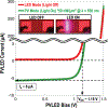
LED and PV modes of operation for AlGaAs PVLED employed in the presented work [20].
Fig. 15.
Fig. 15.
A fully integrated MOTE: (a) a die photograph of an integrated MOTE [20]; (b) simplified cross-sectional view of the MOTE.

Similar articles

Cited by

References

    1. Alivisatos A, Chun M, Church G, Greenspan R, Roukes M and Yuste R, “The brain activity map project and the challenge of functional connectomics,” Neuron, vol. 74, no. 6, pp. 970–974, 2012. - PMC - PubMed
    1. Schenck JF, “The role of magnetic susceptibility in magnetic resonance imaging: MRI magnetic compatibility of the first and second kinds,” Medical Physics, vol. 23, no. 6, pp. 815–850, June 1996. - PubMed
    1. https://www.braininitiative.nih.gov/,” [Online].
    1. Johnson B, Peace ST, Wang A, Cleland TA and Molnar A, “A 768-Channel CMOS Microelectrode Array With Angle Sensitive Pixels for Neuronal Recording,” in lEEESensorsJournal, vol. 13, no. 9, pp. 3211–3218, September 2013.
    1. Dragas J, Viswam V, Shadmani A, Chen Y, Bounik R, Stettler A, Radivojevic M, Geissler S, Obien MEJ, Müller J and Hierlemann A, “In Vitro Multi-Functional Microelectrode Array Featuring 59 760 Electrodes, 2048 Electrophysiology Channels, Stimulation, Impedance Measurement, and Neurotransmitter Detection Channels,” in IEEE Journal of Solid-State Circuits, vol. 52, no. 6, pp. 1576–1590, June 2017. - PMC - PubMed

Publication types