. 2018 Oct 30;9(1):4510.
doi: 10.1038/s41467-018-06760-7.

An electrochemical thermal transistor

Affiliations

An electrochemical thermal transistor

Aditya Sood et al. Nat Commun. .

Erratum in

Abstract

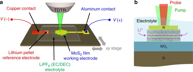
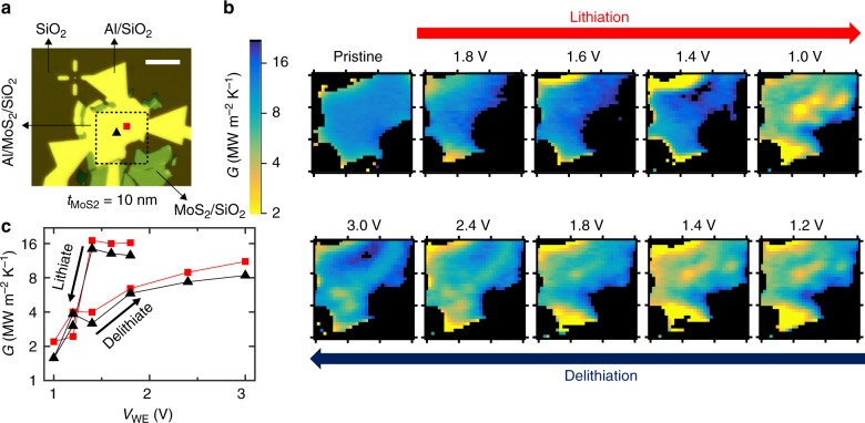
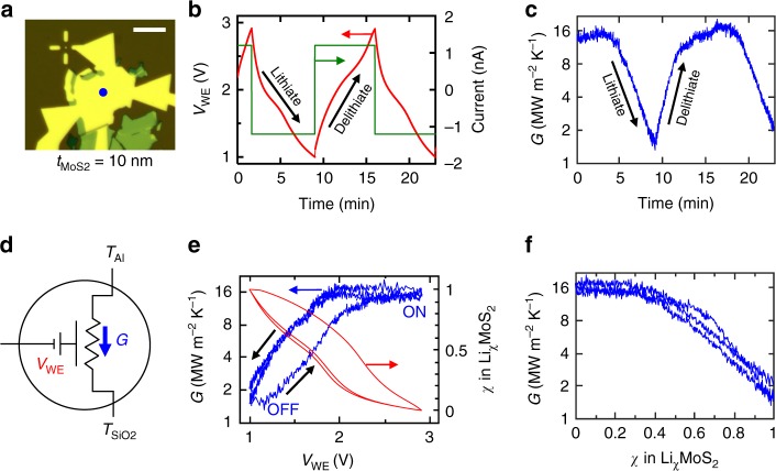
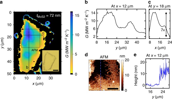
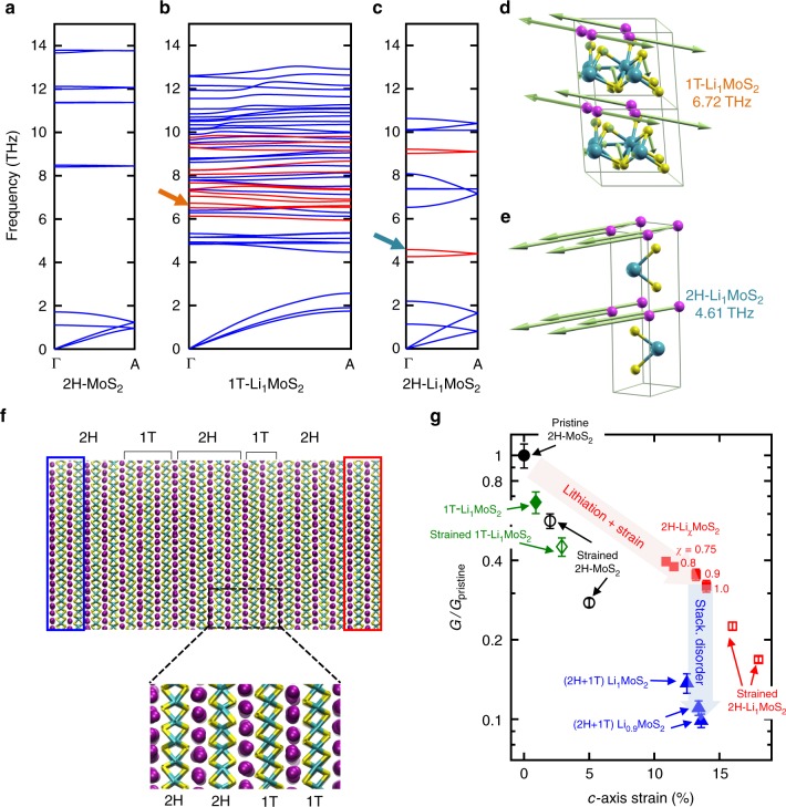
The ability to actively regulate heat flow at the nanoscale could be a game changer for applications in thermal management and energy harvesting. Such a breakthrough could also enable the control of heat flow using thermal circuits, in a manner analogous to electronic circuits. Here we demonstrate switchable thermal transistors with an order of magnitude thermal on/off ratio, based on reversible electrochemical lithium intercalation in MoS2 thin films. We use spatially-resolved time-domain thermoreflectance to map the lithium ion distribution during device operation, and atomic force microscopy to show that the lithiated state correlates with increased thickness and surface roughness. First principles calculations reveal that the thermal conductance modulation is due to phonon scattering by lithium rattler modes, c-axis strain, and stacking disorder. This study lays the foundation for electrochemically-driven nanoscale thermal regulators, and establishes thermal metrology as a useful probe of spatio-temporal intercalant dynamics in nanomaterials.


Conflict of interest statement

The authors declare no competing interests.

Figures

Fig. 1
Fig. 1
Experimental measurement of a thermal transistor. a Schematic of the electrochemical cell used for operando TDTR experiments. b Cross-sectional view of a device under operation. Li ions enter and leave the MoS2 film through the exposed edges
Fig. 2
Fig. 2
Operando scanning thermal conductance imaging. a Optical micrograph of the 10 nm thick MoS2 device. Thermal conductance images are measured within a 15 × 15 µm square region marked by the dotted lines. The scale bar is 10 µm. b Maps of the inhomogeneous thermal conductance within the device taken at different stages of lithiation and delithiation over one electrochemical cycle. These are measured after holding the MoS2 device at a constant potential VWE (relative to Li+/Li) ranging from 1.8 V to 1.0 V for discharging (lithiation) and 1.2 V to 3.0 V for charging (delithiation). c Single-point thermal conductance vs. voltage, tracked over two spots that are indicated in a by the black triangle and red square
Fig. 3
Fig. 3
Thermal transistor characteristics. a Optical micrograph of the device showing the location of real-time TDTR measurements (blue circle). The scale bar is 10 µm. b Galvanostatic characteristics, obtained using an applied (dis)charge current of (−)+1.2 nA (shown in green). The resulting voltage curves are shown in red, taken within fixed limits of 1.0 V and 2.9 V. c Cross-plane thermal conductance measured during the electrochemical cycle shown in b. d Circuit diagram of the thermal transistor device: the gating voltage VWE) that is applied between Li and Al/MoS2 electrodes changes the thermal conductance G) to heat flow between the Al transducer and SiO2 substrate, which are at temperatures TAl and TSiO2 respectively. e Thermal conductance and average lithium composition χ plotted vs. voltage, showing significant hysteresis between charge and discharge curves. f G plotted against χ
Fig. 4
Fig. 4
Ex situ chemical lithiation experiments. a Thermal conductance map of a 72 nm thick single crystal MoS2 film lithiated using n-Butyllithium for 2 h. Inset shows an optical micrograph of the device, after coating with 81 nm thick Al layer (scale bar is 10 µm). b Vertical line scan taken at x = 12 µm, and c horizontal line scan taken at y = 18 µm, extracted from the thermal conductance map along the solid lines marked in a. d AFM image of the region enclosed within the dashed box in a, showing a clear correlation between topography and thermal conductance. The smooth pristine region shows the highest thermal conductance, while the rough lithiated region is more thermally resistive. The scale bar is 5 µm. e Height profile extracted from the AFM image along the blue dashed line indicated in d at x = 12 µm
Fig. 5
Fig. 5
Calculated phonon dispersions along the cross-plane Г-A direction. a 2H-MoS2, b 1T-Li1MoS2, and c 2H-Li1MoS2. Phonon branches are color-coded based on whether they are MoS2-like (blue) or Li-like (red). d, e Force vectors for the modes at 6.72 THz and 4.61 THz in 1T-Li1MoS2 and 2H-Li1MoS2, respectively, showing strong vibrations of Li atoms (depicted by the magenta spheres). f Snapshot of a 10 nm thick NEMD simulation cell showing the mixed phase {4 × 2H, 3 × 1T, 4 × 2H, 2 × 1T, 4 × 2H} Li1MoS2 system, and a zoom-in of a 2H-1T phase boundary. The red and blue boxes are the hot and cold reservoirs, respectively. g NEMD calculations of the normalized cross-plane thermal conductance of a 10 nm thick MoS2 film plotted vs. % c-axis strain, relative to the pristine (unlithiated) 2H-MoS2 (shown as the solid black circle). Red solid squares refer to 2H-LiχMoS2 with χ = 0.75, 0.8, 0.9, and 1, blue solid triangles refer to mixed-phase (2H + 1T) LiχMoS2 with χ = 0.9 and 1 (layer sequences for 2H/1T stacking are provided in the main text), and the green solid diamond refers to 1T-Li1MoS2. In each of the above cases, the c-axis strain is intrinsic, i.e., built into the structure because of Li intercalation. The empty symbols—black circles, red squares, and green diamond—refer to externally strained 2H-MoS2, 2H-Li1MoS2, and 1T-Li1MoS2, respectively. Error bars represent statistical uncertainties arising from the fluctuations of the heat current and the temperature profile at stationary non-equilibrium conditions

References

    1. Sood, A., Pop, E., Asheghi, M. & Goodson, K. E. The heat conduction renaissance. In 17th IEEE Intersociety Conference on Thermal and Thermomechanical Phenomena in Electronic Systems (ITherm) 1396–1402 (IEEE, 2018).
    1. Yan Y, Malen JA. Periodic heating amplifies the efficiency of thermoelectric energy conversion. Energy Environ. Sci. 2013;6:1267–1273. doi: 10.1039/c3ee24158k. - DOI
    1. Wang L, Li B. Thermal logic gates: computation with phonons. Phys. Rev. Lett. 2007;99:177208. doi: 10.1103/PhysRevLett.99.177208. - DOI - PubMed
    1. Li N, et al. Colloquium: phononics: manipulating heat flow with electronic analogs and beyond. Rev. Mod. Phys. 2012;84:1045–1066. doi: 10.1103/RevModPhys.84.1045. - DOI
    1. Walker CT, Pohl RO. Phonon scattering by point defects. Phys. Rev. 1963;131:1433–1442. doi: 10.1103/PhysRev.131.1433. - DOI

Publication types