. 2018 Oct 31;9(1):4546.
doi: 10.1038/s41467-018-06907-6.

Dual-gate organic phototransistor with high-gain and linear photoresponse

Affiliations

Dual-gate organic phototransistor with high-gain and linear photoresponse

Philip C Y Chow et al. Nat Commun. .

Abstract

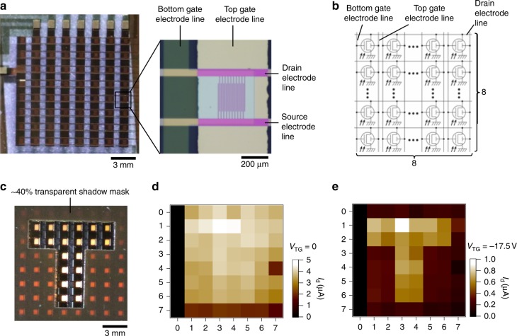
The conversion of light into electrical signal in a photodetector is a crucial process for a wide range of technological applications. Here we report a new device concept of dual-gate phototransistor that combines the operation of photodiodes and phototransistors to simultaneously enable high-gain and linear photoresponse without requiring external circuitry. In an oppositely biased, dual-gate transistor based on a solution-processed organic heterojunction layer, we find that the presence of both n- and p-type channels enables both photogenerated electrons and holes to efficiently separate and transport in the same semiconducting layer. This operation enables effective control of trap carrier density that leads to linear photoresponse with high photoconductive gain and a significant reduction of electrical noise. As we demonstrate using a large-area, 8 × 8 imaging array of dual-gate phototransistors, this device concept is promising for high-performance and scalable photodetectors with tunable dynamic range.


Conflict of interest statement

The authors declare no competing interests

Figures

Fig. 1
Fig. 1
Existing photodetectors and introducing the new device concept of dual-gate phototransistor. ac Schematic illustration and explanatory band diagrams of photodiode, phototransistor, and dual-gate organic phototransistor (with opposite gate biases), respectively. Electron-holes pairs are generated in the semiconducting layer upon light absorption, and are separated to form a photocurrent. Photodiodes can enhance charge separation and collect both carrier types by applying an electric field between the electrodes. Phototransistors only collect one type of carriers by accumulating either electrons or holes at the dielectric-semiconductor interface to form a conductive channel, while the opposite charge remains trapped to allow photoconductive gain. Dual-gate phototransistor consists of two accumulation channels, which can simultaneously conduct opposite charges when the gates are oppositely biased in a sufficiently thick (>10 nm) semiconducting film. The electrostatic interaction between the two accumulation layers introduces an electric field which separates electrons and holes, similar to photodiodes. S/D denotes source and drain electrodes in field-effect transistor architecture. d Dynamic range of a photodetector based on photodiodes (linear photoresponse), phototransistor (sublinear photoresponse with photoconductive gain), and dual-gate phototransistor (linear photoresponse with photoconductive gain until channel saturation). e Device structure of dual-gate phototransistor based on bulk-heterojunction blend of MDMO-PPV and PCBM at 1:15 weight ratio. A self-assembled monolayer of 1-dodecanethiol was formed on the gold source/drain electrodes to improve charge injection. Light is able to reach the photoactive BHJ layer through the semi-transparent ITO/parylene bottom gate. f Top-view optical microscopy image of the device and the electrodes in use. The source/drain electrodes were patterned using lift-off photolithography into a comb-shaped interdigitating pattern, with a total channel width and length of 100 mm and 5 µm, respectively. The effective photoactive area is formed in the overlapping area between the channel and the gate electrodes (red dashed box)
Fig. 2
Fig. 2
Quasi-static optoelectrical characterisation of dual-gate organic phototransistor. a Transfer curves measured in dark at various top gate biases (VTG), with fixed source-drain bias (Vd = 5V). The arrows indicate the scanning direction. The increasing drain current at low VBG indicates the formation of a p channel due to the accumulation of holes at the top dielectric interface when a sufficiently negative VTG is applied, and the threshold voltage shift of the n channel indicates that the two channels are electrostatically interacting. At VBG = 20 V and VTG = −20 V, the drain current is mainly contributed by electrons in the bottom n channel and only partly contributed by holes in the top p channel. b Output curves measured in dark at various top gate biases (VTG), with fixed bottom gate bias (VBG = 20 V). c Transfer curves measured at various light intensities with VTG = 0 V (top) and VTG = -20 V (bottom), at Vd = 5 V. A positive photocurrent (Iphoto) was generated at all gate bias conditions due to the shift in threshold voltage induced by light. Inset shows the output curve in dark (black) and in light (red) at 0.5 mW cm−2 irradiance at VTG = −20 V and VBG = 20 V. d Logarithmic plots showing the dependence of photocurrent (top) and responsivity (bottom) on light intensity (Pin) at both top gate bias conditions (fixed VBG = 20 V). At VTG = 0 V, photocurrent scaled sublinearly with intensity throughout the entire range displayed (IphotoPin-α, with slope α = 0.28 ± 0.03). At VTG = −20 V, photocurrent switched from sublinear dependence at high intensities (> 1 mW cm−2, slope α = 0.32 ± 0.04) to linear dependence at low intensities (< 1 mW cm−2, slope α = 0.97 ± 0.05). The dotted lines show the power-law fits. The linear scaling of photocurrent with light is reflected by the constant high-gain responsivity of about 1 AW−1, which corresponds to an external quantum efficiency (EQE) of ~220% at 543 nm. Similar results were obtained in a dual-gate phototransistor made of DPP-DTT:PCBM blend, but with much-improved performance (~40 AW−1 or ~9000% EQE) due to the enhanced carrier mobility in this blend (see Supplementary Fig. 9)
Fig. 3
Fig. 3
Photodetection performance of dual-gate organic phototransistor. a Transient response of drain current with and without top gate bias (VTG = 0, −20 V), operating at fixed source-drain bias of 5 V and VBG of 20 V. A monochromatic light source was employed for excitation (543 nm, 10 mW cm−2), modulated at 10 Hz using a mechanical chopper. At such high intensity, the twofold increase in photocurrent is likely due to the improved separation of photogenerated electron-hole pairs by the vertical electric field introduced by the oppositely biased gates. b Normalized photocurrent showing the rise and decay kinetics at high (7.5 mW cm−2) and low (0.5 mW cm−2) intensities. At both biases, slower response time was observed at low intensity, which is consistent with the filling of energetically distributed trap states. With negative VTG, slower rise time is likely due to the increase in electron-hole separation by the vertical electric field which extends time taken for the charge trapping/detrapping processes to reach steady state. In dark, the faster decay time can be explained by the sweep out of trapped holes by the top p channel which is not allowed at VTG = 0 V. c Photo-responsivity, noise current spectral density IN and specific detectivity D* as a function of frequency at various VTG. Responsivity, at 1 mW cm−2, was reduced with increasing frequency since it is limited by the response times, and little difference was observed with/without negative VTG. IN also decreased with increasing frequency, showing 1/f characteristics. A significant reduction in IN was observed at increasingly negative VTG (3 orders of magnitude from 0 to −20 V). Such improvement in noise is also reflected in the resulted specific detectivity, which is nearly constant in the displayed frequency range since the reduction in responsivity is compensated by the improved noise. The solid lines serve as guides for the eye
Fig. 4
Fig. 4
Two-dimensional 8 × 8 array of dual-gate organic phototransistors for imaging. a Optical micrograph showing the arrangement of pixels. Each individual pixel has the same structure as shown in Fig. 1e, with channel length and width of 5 µm and 5 mm, respectively. Each column containing 8 pixels shares a common top gate electrode of gold and a common bottom gate electrode of indium tin oxide. b Circuit schematic of the image sensor. c The array was illuminated with white light (1.2 mW cm−2 at 543 nm) through a semi-transparent (~ 40% transmittance at 543 nm), polyimide shadow mask with T-shaped pattern. d At VTG = 0 V, the pattern could not be resolved due to a large background signal (~ 3 µA) caused by light passing through the semi-transparent shadow mask (0.5 mW cm−2). The large background signal is the result of sublinear photoresponse and high level of noise observed in this operation mode. We note that the lack of signal output from column 0 is due to damaged pixels. However, when operating with a negative top gate bias (right), the pattern is clearly imaged (e). The negative top gate bias is limited to −17.5 V (instead of −20 V as demonstrated for individual pixels) in order to reduce cross-talk between pixels from the same column. The improvement in image resolution is due to the reduced noise and linear photoresponse at negative top gate bias, limiting the background signal to only about 0.3 µA in this demonstration

References

    1. Jansen-van Vuuren RD, Armin A, Pandey AK, Burn PL, Meredith P. Organic pPhotodiodes: the future of full color detection and image sensing. Adv. Mater. 2016;28:4766–4802. doi: 10.1002/adma.201505405. - DOI - PubMed
    1. Konstantatos G, Sargent EH. Nanostructured materials for photon detection. Nat. Nanotechnol. 2010;5:391–400. doi: 10.1038/nnano.2010.78. - DOI - PubMed
    1. Ko HC, et al. A hemispherical electronic eye camera based on compressible silicon optoelectronics. Nature. 2008;454:748–753. doi: 10.1038/nature07113. - DOI - PubMed
    1. Baeg KJ, Binda M, Natali D, Caironi M, Noh YY. Organic light detectors: photodiodes and phototransistors. Adv. Mater. 2013;25:4267–4295. doi: 10.1002/adma.201204979. - DOI - PubMed
    1. Gong X, et al. High-detectivity polymer photodetectors with spectral response from 300 nm to 1450 nm. Science. 2009;325:1665–1667. doi: 10.1126/science.1176706. - DOI - PubMed

Publication types