. 2018 Oct 26;4(10):eaat4253.
doi: 10.1126/sciadv.aat4253. eCollection 2018 Oct.

Transistor in a tube: A route to three-dimensional bioelectronics

Affiliations

Transistor in a tube: A route to three-dimensional bioelectronics

C Pitsalidis et al. Sci Adv. .

Abstract

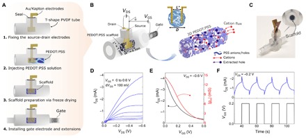
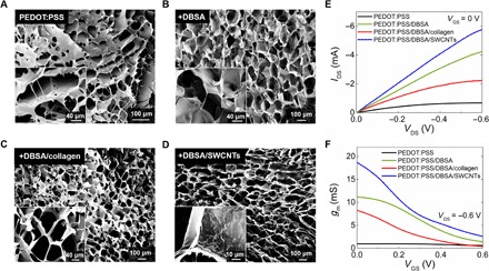
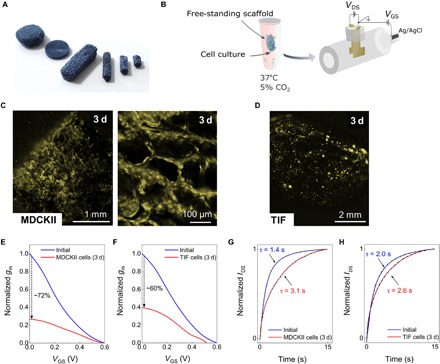
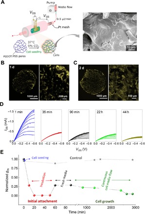
Advances in three-dimensional (3D) cell culture materials and techniques, which more accurately mimic in vivo systems to study biological phenomena, have fostered the development of organ and tissue models. While sophisticated 3D tissues can be generated, technology that can accurately assess the functionality of these complex models in a high-throughput and dynamic manner is not well adapted. Here, we present an organic bioelectronic device based on a conducting polymer scaffold integrated into an electrochemical transistor configuration. This platform supports the dual purpose of enabling 3D cell culture growth and real-time monitoring of the adhesion and growth of cells. We have adapted our system to a 3D tubular geometry facilitating free flow of nutrients, given its relevance in a variety of biological tissues (e.g., vascular, gastrointestinal, and kidney) and processes (e.g., blood flow). This biomimetic transistor in a tube does not require photolithography methods for preparation, allowing facile adaptation to the purpose. We demonstrate that epithelial and fibroblast cells grow readily and form tissue-like architectures within the conducting polymer scaffold that constitutes the channel of the transistor. The process of tissue formation inside the conducting polymer channel gradually modulates the transistor characteristics. Correlating the real-time changes in the steady-state characteristics of the transistor with the growth of the cultured tissue, we extract valuable insights regarding the transients of tissue formation. Our biomimetic platform enabling label-free, dynamic, and in situ measurements illustrates the potential for real-time monitoring of 3D cell culture and compatibility for use in long-term organ-on-chip platforms.


Figures

Fig. 1
Fig. 1. Easy-to-fabricate 3D conducting polymer transistors in a tube: Tubistor.
(A) Schematic representation of the fabrication process. (B) Schematic illustration of the device structure. The device is composed of three main parts: (i) a tubular cavity with three openings (two of these are for the contacts and the gate electrode and the other one is for perfusion), (ii) Au-coated flexible electrodes used as source (S) and drain (D) contacts of the channel fixed inside the tube, and (iii) a PEDOT:PSS scaffold as the channel with the gate electrode embedded inside the tube. To aid with visualization of the channel, a cross-sectional view shows how the electrodes are placed inside the scaffold. The schematic shows the dedoping process inside the channel as cations from the electrolyte are injected into the 3D PEDOT:PSS scaffold. (C) Photograph of a tubistor with a magnified image of the conducting scaffold inside the tube. Photo credit: Charalampos Pitsalidis. (D) Transistor output curves showing the drain current (IDS) as a function of drain voltage (VDS) for a gate voltage (VGS) ranging from 0 to 0.6 V. (E) Transfer characteristics and the corresponding transconductance (gm) of a typical tubistor at VDS = −0.6 V. (F) Transient response of the tubistor to periodic square gate pulses (VGS = 0.2 V for 10 s) at VDS = −0.2 V. The electrolyte was a 0.1 M aqueous NaCl solution. The distance between the source-drain electrodes (L*) in this specific device was approximately 1 mm, while the width (W*) of the scaffold was 4 mm. The diameter (D) of the tubular scaffold was ~1.5 mm.
Fig. 2
Fig. 2. Morphological and electrical characterization of various conducting scaffolds.
SEM images of the tubistors based on (A) neat PEDOT:PSS, (B) PEDOT:PSS/DBSA, (C) PEDOT:PSS/DBSA/collagen, and (D) PEDOT:PSS/DBSA/SWCNT scaffolds. The insets show SEM images of the pores at higher magnification. (E) Comparative output transistor characteristics (at VGS = 0 V) and (F) corresponding transconductance curves for the various types of scaffolds. The transistor characteristics are measured in phosphate-buffered saline (PBS) solution using a Ag/AgCl pellet as the gate electrode. The distance (L*) between the source-drain electrodes was measured to be approximately 1 mm, while the width (W*) of the scaffold in this case was 4 mm. Results shown are from representative devices.
Fig. 3
Fig. 3. Electronic monitoring of ex situ grown 3D cell cultures using tubistor.
(A) Photograph of free-standing PEDOT:PSS scaffolds of various sizes and shapes. Photo credit: Charalampos Pitsalidis. (B) Sketch of the ex situ 3D cell growth and measurement process. Before the electrical measurements, the scaffold was placed in contact with the source-drain electrodes in the presence of culture medium. Fluorescence microscopy image PEDOT:PSS scaffolds seeded with (C) MDCKII and (D) TIF cells after 3 days of cell culture inside an Eppendorf tube. Scanned images were pseudo-colored yellow. Normalized transconductance (gm) versus VGS at VDS = −0.6 V before and after culture with (E) MDCKII and (F) TIF cells. Normalized current response of the OECT to periodic square VGS pulses with and without (G) MDCKII and (H) TIF cells. The dashed black line is the exponential fit used to extract the τ values. The electrical measurements were carried out using a Ag/AgCl gate electrode. The distance (L*) between the source-drain electrodes was measured to be approximately 1.5 mm, while the width (W*) of the scaffold in this set of experiments was 4 mm.
Fig. 4
Fig. 4. Tubistors are compatible with in situ monitoring of cells.
(A) Illustration of the experimental setup used in the dynamic experiments. SEM image showing the MDCKII cells cultured in situ in the PEDOT:PSS scaffold for ~2 days, providing evidence that the cells were able to adhere and form tissue inside the tubistor. The gray line (star points) shows the evolution of transconductance over time of a cell-free device incubated (37°C, 5% CO2) in cell culture medium. Fluorescence images of MDCKII cells cultured in situ for (B) 1 day and (C) 2 days. Scanned images were pseudo-colored yellow. (D) Representative in situ output characteristics of the tubistors recorded during cell growth at various time points. (E) Corresponding evolution of normalized transconductance values at different stages of cell culture process. The electrical measurements were carried out using Pt mesh gate electrode embedded inside the tube extension. The device was connected to an electrical measuring unit during cell culture.

References

    1. Spira M. E., Hai A., Multi-electrode array technologies for neuroscience and cardiology. Nat. Nanotechnol. 8, 83–94 (2013). - PubMed
    1. Heer F., Franks W., Blau A., Taschini S., Ziegler C., Hierlemann A., Baltes H., CMOS microelectrode array for the monitoring of electrogenic cells. Biosens. Bioelectron. 20, 358–366 (2004). - PubMed
    1. Giaever I., Keese C. R., Monitoring fibroblast behavior in tissue culture with an applied electric field. Proc. Natl. Acad. Sci. U.S.A. 81, 3761–3764 (1984). - PMC - PubMed
    1. Fromherz P., Offenhäusser A., Vetter T., Weis J., A neuron-silicon junction: A Retzius cell of the leech on an insulated-gate field-effect transistor. Science 252, 1290–1293 (1991). - PubMed
    1. Rivnay J., Inal S., Salleo A., Owens R. M., Berggren M., Malliaras G. G., Organic electrochemical transistors. Nat. Rev. Mater. 3, 17086 (2018).

Publication types

Substances

LinkOut - more resources