

Custom-Designed Glassy Carbon Tips for Atomic Force Microscopy
- PMID: 30400475
- PMCID: PMC6190046
- DOI: 10.3390/mi8090285
Custom-Designed Glassy Carbon Tips for Atomic Force Microscopy
Abstract
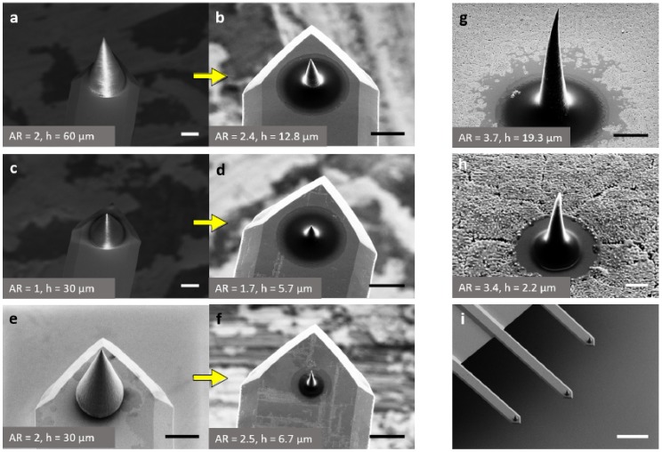
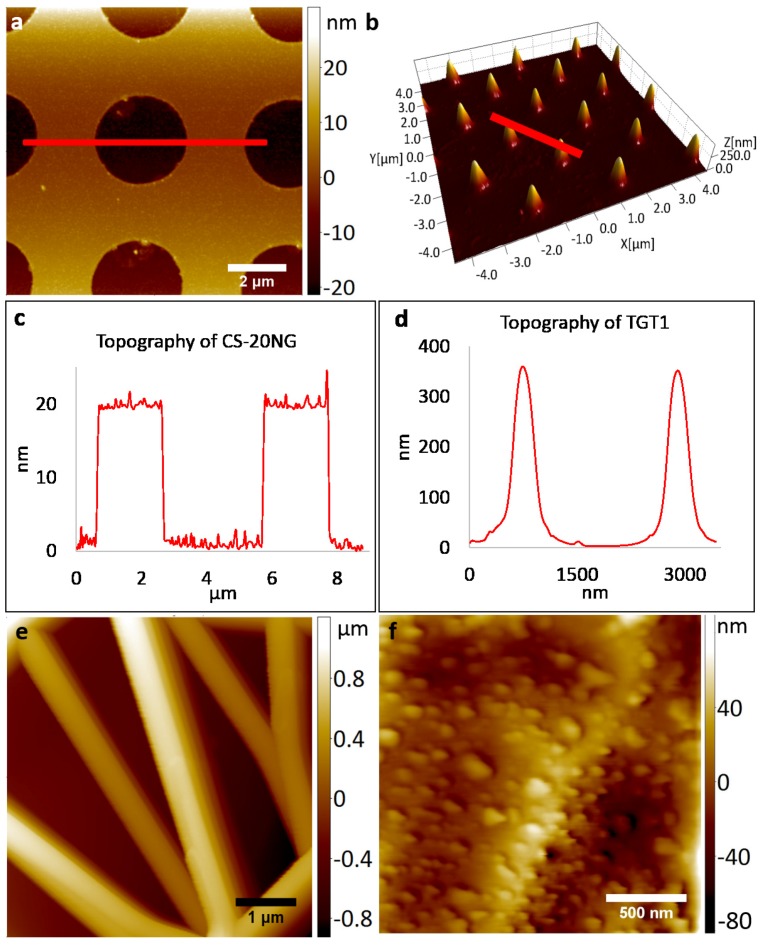
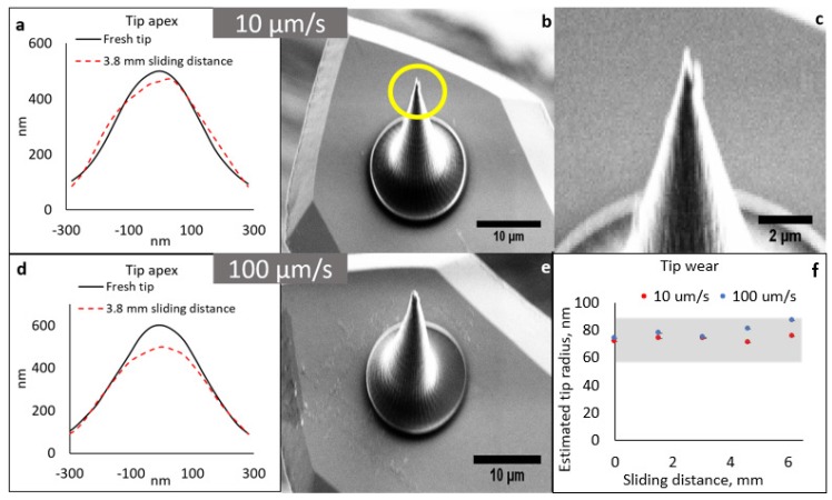
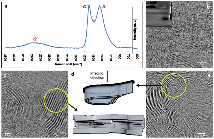
Glassy carbon is a graphenic form of elemental carbon obtained from pyrolysis of carbon-rich precursor polymers that can be patterned using various lithographic techniques. It is electrically and thermally conductive, mechanically strong, light, corrosion resistant and easy to functionalize. These properties render it very suitable for Carbon-microelectromechanical systems (Carbon-MEMS) and nanoelectromechanical systems (Carbon-NEMS) applications. Here we report on the fabrication and characterization of fully operational, microfabricated glassy carbon nano-tips for Atomic Force Microscopy (AFM). These tips are 3D-printed on to micro-machined silicon cantilevers by Two-Photon Polymerization (2PP) of acrylate-based photopolymers (commercially known as IP-series resists), followed by their carbonization employing controlled pyrolysis, which shrinks the patterned structure by ≥98% in volume. Tip performance and robustness during contact and dynamic AFM modes are validated by morphology and wear tests. The design and pyrolysis process optimization performed for this work indicate which parameters require special attention when IP-series polymers are used for the fabrication of Carbon-MEMS and NEMS. Microstructural characterization of the resulting material confirms that it features a frozen percolated network of graphene sheets accompanied by disordered carbon and voids, similar to typical glassy carbons. The presented facile fabrication method can be employed for obtaining a variety of 3D glassy carbon nanostructures starting from the stereolithographic designs provided by the user.
Keywords: AFM tip; Carbon-NEMS; glassy carbon; pyrolysis; two-photon polymerization.
Conflict of interest statement
The authors declare no conflict of interest.
Figures
Similar articles
-
Pyrolysis-induced shrinking of three-dimensional structures fabricated by two-photon polymerization: experiment and theoretical model.Microsyst Nanoeng. 2019 Aug 26;5:38. doi: 10.1038/s41378-019-0079-9. eCollection 2019. Microsyst Nanoeng. 2019. PMID: 31636928 Free PMC article.
-
Evolution of Glassy Carbon Microstructure: In Situ Transmission Electron Microscopy of the Pyrolysis Process.Sci Rep. 2018 Nov 2;8(1):16282. doi: 10.1038/s41598-018-34644-9. Sci Rep. 2018. PMID: 30389995 Free PMC article.
-
Glassy Carbon: A Promising Material for Micro- and Nanomanufacturing.Materials (Basel). 2018 Sep 28;11(10):1857. doi: 10.3390/ma11101857. Materials (Basel). 2018. PMID: 30274225 Free PMC article. Review.
-
Fabrication of 3D Carbon Microelectromechanical Systems (C-MEMS).J Vis Exp. 2017 Jun 17;(124):55649. doi: 10.3791/55649. J Vis Exp. 2017. PMID: 28654068 Free PMC article.
-
Perspectives on C-MEMS and C-NEMS biotech applications.Biosens Bioelectron. 2021 May 15;180:113119. doi: 10.1016/j.bios.2021.113119. Epub 2021 Mar 2. Biosens Bioelectron. 2021. PMID: 33711652 Review.
Cited by
-
Pick and place process for uniform shrinking of 3D printed micro- and nano-architected materials.Nat Commun. 2023 Sep 21;14(1):5876. doi: 10.1038/s41467-023-41535-9. Nat Commun. 2023. PMID: 37735573 Free PMC article.
-
Pyrolysis-induced shrinking of three-dimensional structures fabricated by two-photon polymerization: experiment and theoretical model.Microsyst Nanoeng. 2019 Aug 26;5:38. doi: 10.1038/s41378-019-0079-9. eCollection 2019. Microsyst Nanoeng. 2019. PMID: 31636928 Free PMC article.
-
Evolution of Glassy Carbon Microstructure: In Situ Transmission Electron Microscopy of the Pyrolysis Process.Sci Rep. 2018 Nov 2;8(1):16282. doi: 10.1038/s41598-018-34644-9. Sci Rep. 2018. PMID: 30389995 Free PMC article.
-
Glassy Carbon: A Promising Material for Micro- and Nanomanufacturing.Materials (Basel). 2018 Sep 28;11(10):1857. doi: 10.3390/ma11101857. Materials (Basel). 2018. PMID: 30274225 Free PMC article. Review.
-
Opportunities at the Intersection of 3D Printed Polymers and Pyrolysis for the Microfabrication of Carbon-Based Energy Materials.JACS Au. 2024 Sep 26;4(10):3706-3726. doi: 10.1021/jacsau.4c00555. eCollection 2024 Oct 28. JACS Au. 2024. PMID: 39483227 Free PMC article. Review.
References
-
- Schwarz U.D., Haefke H., Reimann P., Güntherodt H.J. Tip artefacts in scanning force microscopy. J. Microsc. 1994;173:183–197. doi: 10.1111/j.1365-2818.1994.tb03441.x. - DOI
-
- Eaton P., West P. Atomic Force Microscopy. Oxford University Press; Oxford, UK: 2010.
-
- Boisen A., Hansen O., Bouwstra S. AFM probes with directly fabricated tips. J. Micromech. Microeng. 1996;6:58. doi: 10.1088/0960-1317/6/1/012. - DOI
-
- Mesa B., Magonov S. Novel diamond/sapphire probes for scanning probe microscopy applications. J. Phys. Conf. Ser. 2007;61:770–774. doi: 10.1088/1742-6596/61/1/154. - DOI
-
- Neuzil P., Nagarajan R. The formation of sharp AFM tips by single step etching. J. Micromech. Microeng. 2006;16:1298. doi: 10.1088/0960-1317/16/7/025. - DOI
Grants and funding
LinkOut - more resources
Full Text Sources
Miscellaneous
