

Mathematical Modelling and Simulation Research of Thermal Engraving Technology Based on PMMA Material
- PMID: 30407410
- PMCID: PMC6189790
- DOI: 10.3390/mi7030037
Mathematical Modelling and Simulation Research of Thermal Engraving Technology Based on PMMA Material
Abstract
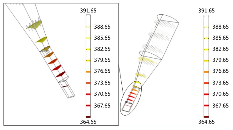
We proposed a thermal engraving technology based on heat transfer theory and polymer rheology in microfluidic field. Then, we established a 3D model of the thermal engraving process based on polymethyl methacrylate (PMMA) material. We could employ the model to analyze the influence of temperature and speed on microchannel processing through the finite element simulation. Thus, we gained the optimal processing parameters. The orthogonal experiments were carried out within the parameter ranges obtained by the simulation results. Finally, we fabricated the smooth microchannel, the average roughness of which was 0.3 μm, by using the optimal parameters. Furthermore, we examined the surface morphology and wettability. Our work provides a convenient technological support for a fast, low-cost, and large-scale manufacturing method of microfluidic chips.
Keywords: MEMS; microchannel; microfluidic chip.
Conflict of interest statement
The authors declare no conflict of interest.
Figures


Similar articles
-
Process Study on 3D Printing of Polymethyl Methacrylate Microfluidic Chips for Chemical Engineering.Micromachines (Basel). 2025 Mar 28;16(4):385. doi: 10.3390/mi16040385. Micromachines (Basel). 2025. PMID: 40283262 Free PMC article.
-
Thermal Effect on Poly(methyl methacrylate) (PMMA) Material Removal in the Micromilling Process.Polymers (Basel). 2020 Sep 17;12(9):2122. doi: 10.3390/polym12092122. Polymers (Basel). 2020. PMID: 32957609 Free PMC article.
-
Research and application of surface heat treatment for CO2 continuous laser ablation of polymeric methyl methacrylate materials.RSC Adv. 2024 Jan 8;14(3):1909-1923. doi: 10.1039/d3ra05391a. eCollection 2024 Jan 3. RSC Adv. 2024. PMID: 38192322 Free PMC article.
-
Fabrication of Spiral Low-Cost Microchannel with Trapezoidal Cross Section for Cell Separation Using a Grayscale Approach.Micromachines (Basel). 2023 Jun 30;14(7):1340. doi: 10.3390/mi14071340. Micromachines (Basel). 2023. PMID: 37512651 Free PMC article.
-
[Laboratory on a microfluidic chip].Se Pu. 2005 Sep;23(5):456-63. Se Pu. 2005. PMID: 16350786 Review. Chinese.
References
-
- Ren M.Y., Tian L. Design and simulation of photoelectric detection circuit for microfluidics chip. Appl. Mech. Mater. 2013;384:3308–3311. doi: 10.4028/www.scientific.net/AMM.380-384.3308. - DOI
-
- Matteucci M., Christiansen T.L. Fabrication and characterization of injection molded multi level nano and microfluidic systems. Microelectron. Eng. 2013;111:294–298. doi: 10.1016/j.mee.2013.01.060. - DOI
-
- Nugen S.R., Asiello P.J. Design and fabrication of a microfluidic device for near-single cell mRNA isolation using a copper hot embossing master. Microsyst. Technol. 2009;15:477–483. doi: 10.1007/s00542-008-0694-0. - DOI
LinkOut - more resources
Full Text Sources
