

Electroosmotic Flow in Microchannel with Black Silicon Nanostructures
- PMID: 30424162
- PMCID: PMC6187698
- DOI: 10.3390/mi9050229
Electroosmotic Flow in Microchannel with Black Silicon Nanostructures
Abstract
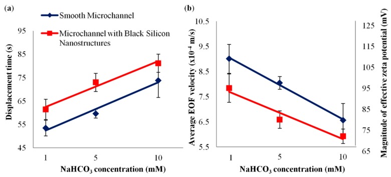
Although electroosmotic flow (EOF) has been applied to drive fluid flow in microfluidic chips, some of the phenomena associated with it can adversely affect the performance of certain applications such as electrophoresis and ion preconcentration. To minimize the undesirable effects, EOF can be suppressed by polymer coatings or introduction of nanostructures. In this work, we presented a novel technique that employs the Dry Etching, Electroplating and Molding (DEEMO) process along with reactive ion etching (RIE), to fabricate microchannel with black silicon nanostructures (prolate hemispheroid-like structures). The effect of black silicon nanostructures on EOF was examined experimentally by current monitoring method, and numerically by finite element simulations. The experimental results showed that the EOF velocity was reduced by 13 ± 7%, which is reasonably close to the simulation results that predict a reduction of approximately 8%. EOF reduction is caused by the distortion of local electric field at the nanostructured surface. Numerical simulations show that the EOF velocity decreases with increasing nanostructure height or decreasing diameter. This reveals the potential of tuning the etching process parameters to generate nanostructures for better EOF suppression. The outcome of this investigation enhances the fundamental understanding of EOF behavior, with implications on the precise EOF control in devices utilizing nanostructured surfaces for chemical and biological analyses.
Keywords: current monitoring method; electroosmotic flow; finite element method; injection molding; micro-/nanofabrication; reactive ion etching.
Conflict of interest statement
The authors declare no conflict of interest.
Figures


References
-
- Lim C.Y., Lam Y.C. Analysis on micro-mixing enhancement through a constriction under time periodic electroosmotic flow. Microfluid. Nanofluid. 2012;12:127–141. doi: 10.1007/s10404-011-0856-8. - DOI
-
- Chang C.C., Yang R.J. Electrokinetic mixing in microfluidic systems. Microfluid. Nanofluid. 2007;3:501–525. doi: 10.1007/s10404-007-0178-z. - DOI
Grants and funding
LinkOut - more resources
Full Text Sources
