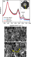
Laser-Induced Periodic Surface Structures (LIPSS) on Heavily Boron-Doped Diamond for Electrode Applications
- PMID: 30431259
- PMCID: PMC6326536
- DOI: 10.1021/acsami.8b15951
Laser-Induced Periodic Surface Structures (LIPSS) on Heavily Boron-Doped Diamond for Electrode Applications
Abstract
Diamond is known as a promising electrode material in the fields of cell stimulation, energy storage (e.g., supercapacitors), (bio)sensing, catalysis, etc. However, engineering its surface and electrochemical properties often requires costly and complex procedures with addition of foreign material (e.g., carbon nanotube or polymer) scaffolds or cleanroom processing. In this work, we demonstrate a novel approach using laser-induced periodic surface structuring (LIPSS) as a scalable, versatile, and cost-effective technique to nanostructure the surface and tune the electrochemical properties of boron-doped diamond (BDD). We study the effect of LIPSS on heavily doped BDD and investigate its application as electrodes for cell stimulation and energy storage. We show that quasi-periodic ripple structures formed on diamond electrodes laser-textured with a laser accumulated fluence of 0.325 kJ/cm2 (800 nm wavelength) displayed a much higher double-layer capacitance of 660 μF/cm2 than the as-grown BDD (20 μF/cm2) and that an increased charge-storage capacity of 1.6 mC/cm2 (>6-fold increase after laser texturing) and a low impedance of 2.74 Ω cm2 turn out to be appreciable properties for cell stimulation. Additional morphological and structural characterization revealed that ripple formation on heavily boron-doped diamond (2.8 atom % [B]) occurs at much lower accumulated fluences than the 2 kJ/cm2 typically reported for lower doping levels and that the process involves stronger graphitization of the BDD surface. Finally, we show that the exposed interface between sp2 and sp3 carbon layers (i.e. the laser-ablated diamond surface) revealed faster kinetics than the untreated BDD in both ferrocyanide and RuHex mediators, which can be used for electrochemical (bio)sensing. Overall, our work demonstrates that LIPSS is a powerful single-step tool for the fabrication of surface-engineered diamond electrodes with tunable material, electrochemical, and charge-storage properties.
Keywords: LIPSS; boron-doped diamond; charge-storage capacity; cyclic voltammetry; impedance spectroscopy; laser texturing; ripples; supercapacitor.
Conflict of interest statement
The authors declare no competing financial interest.
Figures


Similar articles
-
Surface Nanotexturing of Boron-Doped Diamond Films by Ultrashort Laser Pulses.Micromachines (Basel). 2023 Feb 4;14(2):389. doi: 10.3390/mi14020389. Micromachines (Basel). 2023. PMID: 36838089 Free PMC article.
-
Boron-Doped Diamond Electrodes: Fundamentals for Electrochemical Applications.Acc Chem Res. 2022 Dec 20;55(24):3605-3615. doi: 10.1021/acs.accounts.2c00597. Epub 2022 Dec 7. Acc Chem Res. 2022. PMID: 36475616
-
Inkjet Printing-Manufactured Boron-Doped Diamond Chip Electrodes for Electrochemical Sensing Purposes.ACS Appl Mater Interfaces. 2023 Aug 23;15(33):39915-39925. doi: 10.1021/acsami.3c04824. Epub 2023 Aug 9. ACS Appl Mater Interfaces. 2023. PMID: 37556596 Free PMC article.
-
Electrogenerated chemiluminescence at boron-doped diamond electrodes.Chem Commun (Camb). 2023 Jun 22;59(51):7900-7910. doi: 10.1039/d3cc01507f. Chem Commun (Camb). 2023. PMID: 37249438 Review.
-
Boron-doped diamond nano/microelectrodes for biosensing and in vitro measurements.Front Biosci (Schol Ed). 2011 Jan 1;3(2):518-40. doi: 10.2741/s169. Front Biosci (Schol Ed). 2011. PMID: 21196394 Free PMC article. Review.
Cited by
-
Sub-diffraction limited nanogroove fabrication of 30 nm features on diamond films using 800 nm femtosecond laser irradiation.Heliyon. 2024 Jan 9;10(2):e24240. doi: 10.1016/j.heliyon.2024.e24240. eCollection 2024 Jan 30. Heliyon. 2024. PMID: 38304800 Free PMC article.
-
The Fabrication of Micro/Nano Structures by Laser Machining.Nanomaterials (Basel). 2019 Dec 16;9(12):1789. doi: 10.3390/nano9121789. Nanomaterials (Basel). 2019. PMID: 31888222 Free PMC article. Review.
-
LIPSS Applied to Wide Bandgap Semiconductors and Dielectrics: Assessment and Future Perspectives.Materials (Basel). 2022 Feb 13;15(4):1378. doi: 10.3390/ma15041378. Materials (Basel). 2022. PMID: 35207919 Free PMC article.
-
Templated Synthesis of Diamond Nanopillar Arrays Using Porous Anodic Aluminium Oxide (AAO) Membranes.Nanomaterials (Basel). 2023 Feb 27;13(5):888. doi: 10.3390/nano13050888. Nanomaterials (Basel). 2023. PMID: 36903765 Free PMC article.
-
Mechanism of Defect-Impurity Synergy in Laser-Induced Conductive Layer on Single-Crystal Diamond Surfaces.ACS Omega. 2025 Aug 1;10(31):35278-35284. doi: 10.1021/acsomega.5c05740. eCollection 2025 Aug 12. ACS Omega. 2025. PMID: 40821539 Free PMC article.
References
-
- Gicquel A.; Hassouni K.; Silva F.; Achard J. CVD Diamond Films: From Growth to Applications. Curr. Appl. Phys. 2001, 1, 479–496. 10.1016/S1567-1739(01)00061-X. - DOI
-
- Nebel C. E. Electronic Properties of CVD Diamond. Semicond. Sci. Technol. 2003, 18, S1–S11. 10.1088/0268-1242/18/3/301. - DOI
-
- Szunerits S.; Nebel C. E.; Hamers R. J. Surface Functionalization and Biological Applications of CVD Diamond. MRS Bull. 2014, 39, 517–524. 10.1557/mrs.2014.99. - DOI
-
- Childress L.; Hanson R. Diamond NV Centers for Quantum Computing and Quantum Networks. MRS Bull. 2013, 38, 134–138. 10.1557/mrs.2013.20. - DOI
-
- Riedrich-Möller J.; Kipfstuhl L.; Hepp C.; Neu E.; Pauly C.; Mucklich F.; Baur A.; Wandt M.; Wolff S.; Fischer M.; Gsell S.; Schreck M.; Becher C. One- and Two-Dimensional Photonic Crystal Microcavities in Single Crystal Diamond. Nat. Nanotechnol. 2012, 7, 69–74. 10.1038/nnano.2011.190. - DOI - PubMed
LinkOut - more resources
Full Text Sources

