. 2018 Nov 15;9(1):4801.
doi: 10.1038/s41467-018-07279-7.

Parity transitions in the superconducting ground state of hybrid InSb-Al Coulomb islands

Affiliations

Parity transitions in the superconducting ground state of hybrid InSb-Al Coulomb islands

Jie Shen et al. Nat Commun. .

Abstract

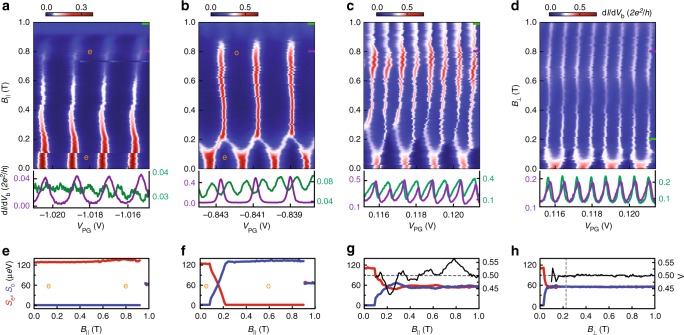
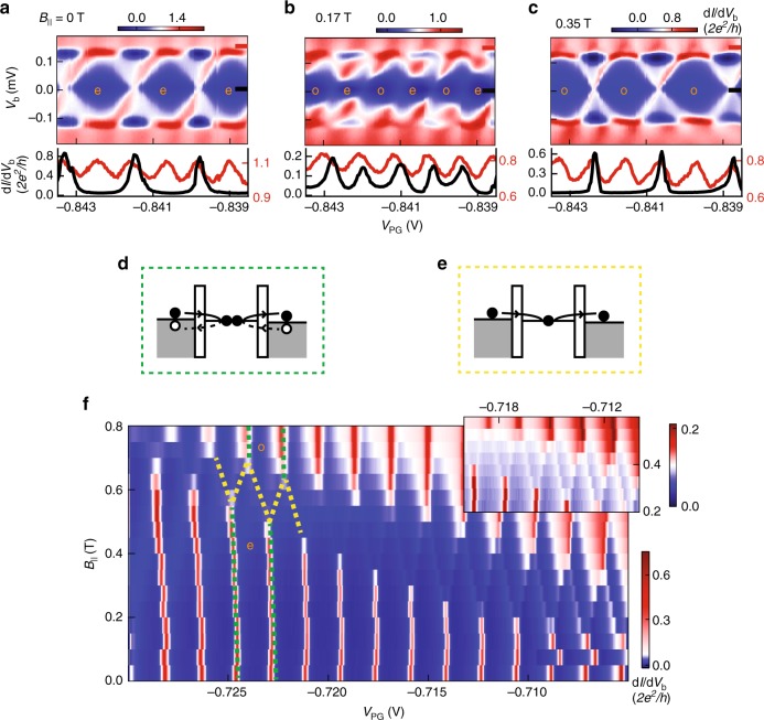
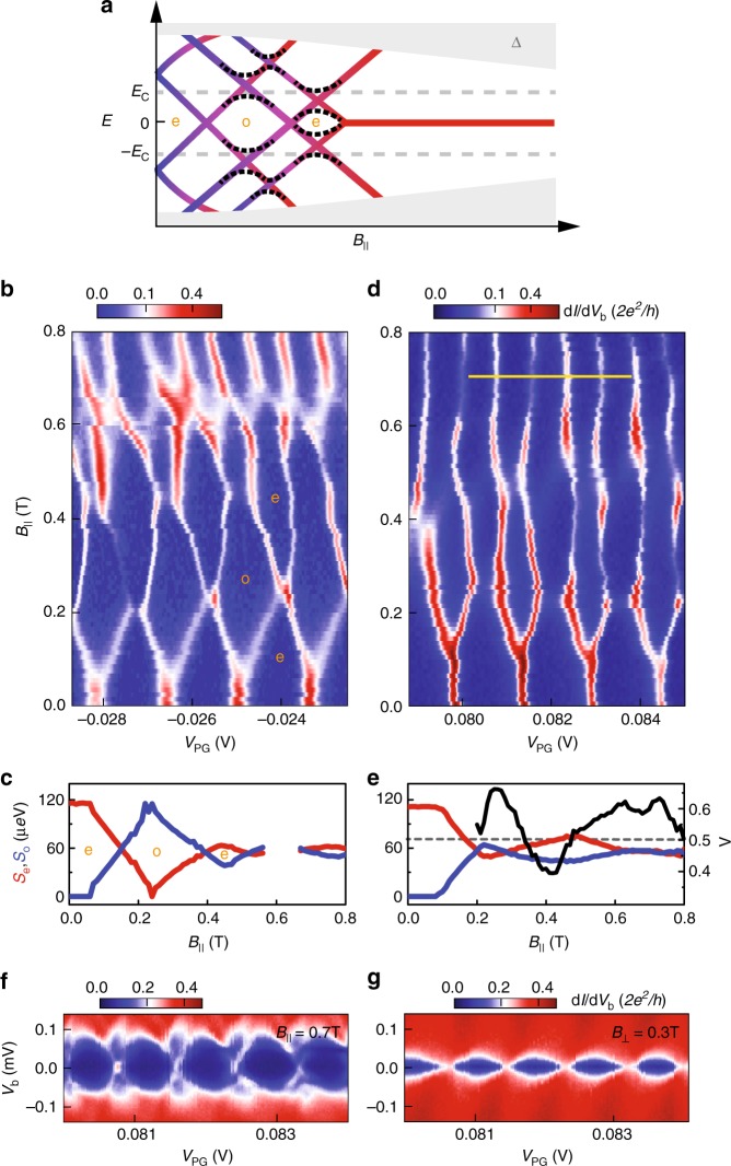
The number of electrons in small metallic or semiconducting islands is quantised. When tunnelling is enabled via opaque barriers this number can change by an integer. In superconductors the addition is in units of two electron charges (2e), reflecting that the Cooper pair condensate must have an even parity. This ground state (GS) is foundational for all superconducting qubit devices. Here, we study a hybrid superconducting-semiconducting island and find three typical GS evolutions in a parallel magnetic field: a robust 2e-periodic even-parity GS, a transition to a 2e-periodic odd-parity GS, and a transition from a 2e- to a 1e-periodic GS. The 2e-periodic odd-parity GS persistent in gate-voltage occurs when a spin-resolved subgap state crosses zero energy. For our 1e-periodic GSs we explicitly show the origin being a single zero-energy state gapped from the continuum, i.e., compatible with an Andreev bound states stabilized at zero energy or the presence of Majorana zero modes.


Conflict of interest statement

The authors declare no competing interests.

Figures

Fig. 1
Fig. 1
Hybrid semiconducting–superconducting island and its energy spectrum. a False-colour scanning electron microscope image of the device consisting of an InSb nanowire (green) with an 800–900 nm long Al-shell (light-blue) covering the top facet and one side facet. Inset: schematic cross-section at the centre of the plunger gate (PG) indicated by the yellow line. The Si/SiOx substrate contains a global back gate that we keep at zero voltage. The InSb wire is contacted by Cr/Au leads (yellow) and then covered by a 30 nm-thick dielectric layer of SiNx (light-grey). Ti/Au top gates (blue) that wrap around the wire allow for local electrostatic control of the electron density. Two gates are used to induce tunnel barriers (TG) and one plunger gate (PG) controls the electron number on the island. The scale bar indicates 500 nm. b dI/dVb vs. tunnel gate voltage and Vb showing 2e-periodic Coulomb diamonds (one diamond is outlined by yellow dashed lines). The lower panel shows horizontal linecuts with 2e-periodic Coulomb oscillations at Vb = 0 (black trace) and 1e-periodic oscillations at Vb = 150 μV (red trace). The panel on the right shows a vertical linecut through the Coulomb peak at the degeneracy point (blue trace) and through the centre of the Coulomb diamond (purple trace). Below are four scenarios for the B-dependence of a single Andreev level (cf), the resulting energies as a function of the induced charge, Ng (gj), and the Coulomb oscillations (kn). In panels cf, the grey regions represent the continuum of states above ∆. The coloured traces represent the energy, E0, of the lowest-energy subgap state. Panels gj show the energies of the island with N excess electrons, E(Ng) = Ec(Ng − N)2 + pNE0, where Ng is the gate-induced charge, N is the electron occupancy number, and pN = 0 (1) for N = even (odd). Parabolas for N = even are shown in black, while parabolas for N = odd are shown in colours in correspondence to the colours in the other rows. Crossings in the lowest-energy parabolas correspond to Coulomb peaks as sketched in panels kn, again with the same colour coding. Labels in the Coulomb valleys between the peaks indicate the GS parity being either even (e) or odd (o)
Fig. 2
Fig. 2
Four representative evolutions of Coulomb peaks, corresponding to the four columns (cn) in Fig. 1. Top row panels: dI/dVb as a function of VPG and B (ac) or B (d). Below are typical linecuts at different B-fields indicated by the purple and green lines. (eh) Even and odd peak spacings, Se (red) and So (blue) on the left axis, and peak height ratio, Λ (black) on the right axis, vs. B-field, for the valleys labelled e/o in a and b and for the average spacings in c and d, respectively. Here and in other figures, the linewidths of Se and So curves correspond to 5 µeV, in accordance with the lock-in excitation energy. a The 2e-periodicity with even-parity valleys persists up to 0.9 T, above which quasiparticle poisoning occurs. b The 2e-periodic peaks split at ~0.11 T and merge again at ~0.23 T. For B > 0.23 T, the oscillations are again 2e-periodic, but here the GS parity is odd, consistent with Fig. 1h. c 2e-periodicity transitioning to uniform 1e-periodicity at B ≈ 0.35 T, accompanied by peak spacing and peak height ratio oscillations up to 0.9 T (see also panel g). d 2e-periodicity transitioning to 1e-periodicity at B = 0.18 T (the vertical dashed line), coinciding with the critical B-field of the Al layer (see Supplementary Fig. 3). Above the critical field, peak heights are constant (see linecuts) and the even/odd peak spacings are equal (h). A few common offsets in VPG are introduced to compensate the shifts in gate voltage, and the raw data are listed in Supplementary Fig. 4
Fig. 3
Fig. 3
Transport via an odd-parity GS. (ac) Coulomb diamonds for the gate settings in Fig. 2b at different B. Below are linecuts at Vb = 0 (black trace) and Vb = 150 μV (red trace), respectively. f Another example of an even-to-odd GS transition. The inset is a zoom-in of the even–odd regime with a different scale bar. The sketch in d illustrates the Cooper pair tunnelling process in both even- and odd-GS regimes (marked by green dashed lines in f), while e illustrates the single electron tunnelling process in the alternating even–odd parity GS regime (marked by yellow dashed lines in f)
Fig. 4
Fig. 4
Evolution of multiple subgap states. a Schematic B-field dependence for the case of three subgap states with GS parity transitions at each zero-energy crossing. Dashed lines indicate level repulsion between different subgap states, leading to large oscillations of the lowest energy E0. b One example of Coulomb peaks reflected by the scenario in panel a. The extracted peak spacings for the valleys labelled by e and o are shown below in c. The evolution of the peak spacings is compatible with the type of energy spectrum shown in a characterised by large oscillations of E0. Note that the odd-parity GS around ~0.2 T develops a full 2e-periodicity. (The spacings near ~0.6 T are absent because the exact peak positions are unclear.) d Another example of Coulomb oscillations with a pronounced B-field dependence. Extracted peak spacings and the height ratio are shown in e (averaged over the three periods in d). f Coulomb diamonds at B = 0.7 T along the VPG-range indicated by the yellow line in d. This bias spectroscopy reveals isolated zero-bias peaks at the charge-degeneracy points that are separated from the continuum. As in Fig. 2c, neighbouring zero-bias peaks have different heights (also visible in d at high B). g Bias spectroscopy with Al in the normal state (B = 0.3 T) where the isolated zero-bias peaks are absent

References

    1. Lutchyn RM, Sau JD, Das Sarma S. Majorana fermions and a topological phase transition in semiconductor-superconductor heterostructures. Phys. Rev. Lett. 2010;105:077001. doi: 10.1103/PhysRevLett.105.077001. - DOI - PubMed
    1. Oreg Y, Refael G, von Oppen F. Helical liquids and Majorana bound states in quantum wires. Phys. Rev. Lett. 2010;105:177002. doi: 10.1103/PhysRevLett.105.177002. - DOI - PubMed
    1. Fu L. Electron teleportation via Majorana bound states in a mesoscopic superconductor. Phys. Rev. Lett. 2010;104:056402. doi: 10.1103/PhysRevLett.104.056402. - DOI - PubMed
    1. Das Sarma S, Freedman M, Nayak C. Majorana zero modes and topological quantum computation. Npj Quantum Inf. 2015;1:15001. doi: 10.1038/npjqi.2015.1. - DOI
    1. Kouwenhoven, L. P. et al. Electron transport in quantum dots. In Mesoscopic Electron Transport, Vol. 345, 105 (Springer, Dordrecht, 1997).

Publication types