. 2018 Dec 12;18(12):7969-7976.
doi: 10.1021/acs.nanolett.8b03937. Epub 2018 Nov 30.

Strain-Tunable Quantum Integrated Photonics

Affiliations

Strain-Tunable Quantum Integrated Photonics

Ali W Elshaari et al. Nano Lett. .

Abstract

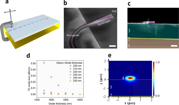
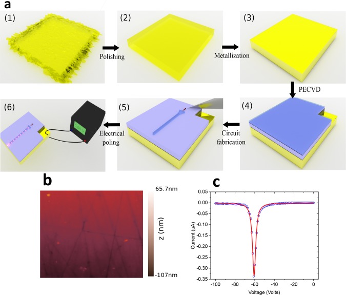
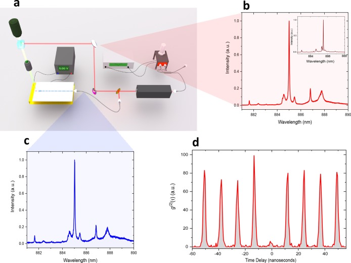
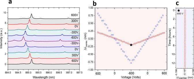
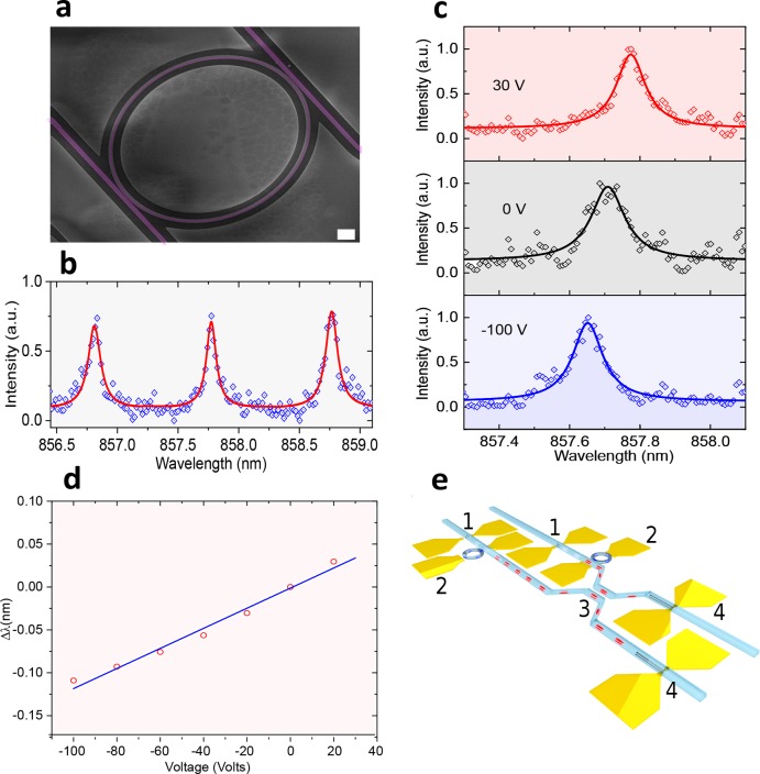
Semiconductor quantum dots are crucial parts of the photonic quantum technology toolbox because they show excellent single-photon emission properties in addition to their potential as solid-state qubits. Recently, there has been an increasing effort to deterministically integrate single semiconductor quantum dots into complex photonic circuits. Despite rapid progress in the field, it remains challenging to manipulate the optical properties of waveguide-integrated quantum emitters in a deterministic, reversible, and nonintrusive manner. Here we demonstrate a new class of hybrid quantum photonic circuits combining III-V semiconductors, silicon nitride, and piezoelectric crystals. Using a combination of bottom-up, top-down, and nanomanipulation techniques, we realize strain tuning of a selected, waveguide-integrated, quantum emitter and a planar integrated optical resonator. Our findings are an important step toward realizing reconfigurable quantum-integrated photonics, with full control over the quantum sources and the photonic circuit.

Keywords: Nanowires; quantum dot; quantum integrated photonics; ring resonator; single photon; strain tuning.


Conflict of interest statement

The authors declare no competing financial interest.

Figures

Figure 1
Figure 1
(a) Artistic representation of a waveguide-coupled nanowire single-photon source, directly fabricated on a strain-tunable substrate. (b) Scanning electron microscope image of an InP nanowire QD, shown in red, coupled to a silicon nitride waveguide, shown in purple, all directly fabricated on the PMN–PT substrate. (c) Scanning electron microscope image of the waveguide cross section. The different layers from bottom to top are PMN–PT crystal (labeled “1”), 20 nm of chromium and 80 nm of gold (labeled “2”), 2 μm of silicon oxide (labeled “3”), and 230 nm of silicon nitride (labeled “4”). (d) Numerical simulations of the fundamental TE mode loss as a function of the silicon oxide cladding thickness and the silicon nitride core thickness. (e) Electric-field profile of the fundamental TE mode showing no significant plasmonic coupling to the bottom gold contact; the silicon nitride thickness is 230 nm and the silicon oxide thickness is 2 μm. The scale bars in panels b and c are 2 and 1 μm, respectively.
Figure 2
Figure 2
(a) Process flow for fabricating the device: (1) Raw PMN–PT substrate with rough surface, which is initially not suitable for fabricating photonic circuits due to the deep trenches formed during ingot sawing. (2) Polished PMN–PT chip. (3) Metal evaporation to form top and bottom contacts. (4) Deposition of silicon oxide and silicon nitride using plasma-enhanced chemical vapor. 1 mm2 of the gold surface is left exposed for subsequent electrical bonding. (5) Electron beam lithography and reactive ion etching to form different photonic elements, then deterministic placement of a selected nanowire quantum dot using nanomanipulation technique. (6) Poling of the piezo using a high-voltage source, then optical and electrical testing. (b) Atomic force microscope image of the polished piezo surface with an RMS roughness of 22.5 nm. (c) Electrical poling curve of the processed piezoelectric chip at room temperature. Despite extensive processing steps, including electron-beam lithography, thin-film deposition, and reactive ion etching, no visible degradation in the piezoelectric behavior of the crystal is seen.
Figure 3
Figure 3
(a) Experimental setup for the piezo-tunable hybrid quantum photonic circuit. The setup allows for both in-plane (via the waveguide using tapered optical fiber) and out-of-plane laser excitation and collection; additional details of the setup are available in the main text. The collected emission from the nanowire QD is coupled to a monochromator, then either detected by charge-coupled devices camera or fiber-coupled to two superconducting single-photon detectors and a correlation module. The QD is nonresonantly excited with 3 ps pulsed laser operating at 795 nm wavelength. (b,c) Out-of-plane (free space) and through the waveguide (via optical fiber) collected emission spectrum of the QD, respectively. The inset in panel b shows the same QD emission at the growth chip before transfer. (d) Second-order correlation measurement of the QD line at ∼885 nm; the uncorrected zero-delay multiphoton probability is g(2)(0) = 0.1 ± 0.04, showing the nonclassical nature of the deterministically integrated quantum emitter.
Figure 4
Figure 4
(a) Emission spectra of the nanowire QD collected from the waveguide as a function of the applied voltage to the piezoelectric substrate. Negative voltages correspond to compressive biaxial strain, resulting in lowering the emission energy of the QD. We achieve a total shift in the QD emission of 0.39 nm by changing the applied voltage to the piezoelectric substrate by 1.2 kV. (b) Red circles show the trace of a single fitted peak of the QD emission as a function of the applied voltage; we see a clear linear and recoverable behavior for the QD tuning. The strain transfer between the nanowire QD and the substrate is mainly due to van der Waals forces between the two. The tunability can be enhanced by increasing the surface area of the interaction region between the two and anchoring the nanowire rigidly to the substrate. To achieve this, we deposited 20 nm of silicon nitride and 200 nm of silicon oxide using plasma-enhanced chemical vapor; the tuning results are shown in blue circles in panel b. After deposition, we achieve a four-fold increase in the strain transfer; the total shift of the QD emission after encapsulation is 1.6 nm. (c) Emission stability test. The piezo voltage was fixed at −600 V while measuring the spectrum every 1 min for 13 h. The emission wavelength shows excellent stability, with no measurable shift within the experimental setup resolution of 25 μeV.
Figure 5
Figure 5
(a) Scanning electron microscope image of silicon nitride ring resonator fabricated on a piezoelectric substrate, the scale bar is 2 μm. (b) Drop port transmission of the ring resonator with free spectral range of 0.96 nm. (c) Single resonance peak at different applied voltages to the PMPT–PT substrate: 30, 0, and −100 V for top, middle, and bottom panels, respectively. Negative voltages correspond to compressive biaxial strain, resulting in blue-shifting the resonance of the optical cavity. (d) Trace of the drop port transmission peak as a function of voltage. (e) Envisioned applications of strain-tunable hybrid quantum photonic circuit. The depicted circuit shows two nanowire quantum emitters (labeled “1”) strain-tuned to the same wavelength, then a filtering stage consisting of a pair of ring resonators (labeled “2”) that are strain-tuned to transmit specific optical transitions of the nanowire QD. Finally, a pair of superconducting nanowire single-photon detectors (labeled “4”) is integrated with a beam splitter (labeled “3”) to study on-chip quantum interference between remote emitters.

References

    1. Bouwmeester D.; Pan J.-W.; Mattle K.; Eibl M.; Weinfurter H.; Zeilinger A. Nature 1997, 390 (6660), 575–579. 10.1038/37539. - DOI
    1. Aspect A.; Dalibard J.; Roger G. Phys. Rev. Lett. 1982, 49 (25), 1804. 10.1103/PhysRevLett.49.1804. - DOI
    1. Akopian N.; Lindner N. H.; Poem E.; Berlatzky Y.; Avron J.; Gershoni D.; Gerardot B. D.; Petroff P. M. Phys. Rev. Lett. 2006, 96 (13), 130501. 10.1103/PhysRevLett.96.130501. - DOI - PubMed
    1. Wakabayashi R.; Fujiwara M.; Yoshino K.-i.; Nambu Y.; Sasaki M.; Aoki T. Opt. Express 2015, 23 (2), 1103–1103. 10.1364/OE.23.001103. - DOI - PubMed
    1. Jayakumar H.; Predojević A.; Kauten T.; Huber T.; Solomon G. S.; Weihs G. Nat. Commun. 2014, 5, 4251. 10.1038/ncomms5251. - DOI - PMC - PubMed

Publication types