

Metal-to-Semiconductor Transition and Electronic Dimensionality Reduction of Ca2N Electride under Pressure
- PMID: 30479920
- PMCID: PMC6247025
- DOI: 10.1002/advs.201800666
Metal-to-Semiconductor Transition and Electronic Dimensionality Reduction of Ca2N Electride under Pressure
Abstract
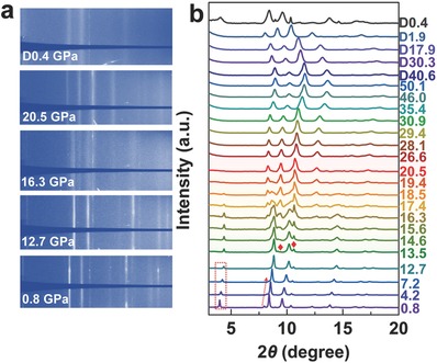
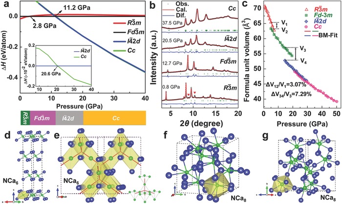
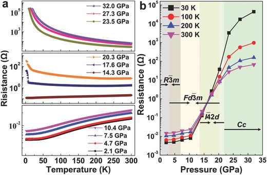
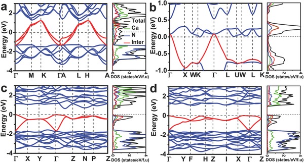
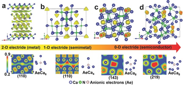
The discovery of electrides, in particular, inorganic electrides where electrons substitute anions, has inspired striking interests in the systems that exhibit unusual electronic and catalytic properties. So far, however, the experimental studies of such systems are largely restricted to ambient conditions, unable to understand their interactions between electron localizations and geometrical modifications under external stimuli, e.g., pressure. Here, pressure-induced structural and electronic evolutions of Ca2N by in situ synchrotron X-ray diffraction and electrical resistance measurements, and density functional theory calculations with particle swarm optimization algorithms are reported. Experiments and computation are combined to reveal that under compression, Ca2N undergoes structural transforms from R m symmetry to I 2d phase via an intermediate Fd m phase, and then to Cc phase, accompanied by the reductions of electronic dimensionality from 2D, 1D to 0D. Electrical resistance measurements support a metal-to-semiconductor transition in Ca2N because of the reorganizations of confined electrons under pressure, also validated by the calculation. The results demonstrate unexplored experimental evidence for a pressure-induced metal-to-semiconductor switching in Ca2N and offer a possible strategy for producing new electrides under moderate pressure.
Keywords: electrides; electronic dimensionality; metal‐to‐insulator transition; phase evolution.
Figures
Similar articles
-
Pressure-Stabilized Semiconducting Electrides in Alkaline-Earth-Metal Subnitrides.J Am Chem Soc. 2017 Oct 4;139(39):13798-13803. doi: 10.1021/jacs.7b07016. Epub 2017 Sep 22. J Am Chem Soc. 2017. PMID: 28898056
-
Electron Confinement in Channel Spaces for One-Dimensional Electride.J Phys Chem Lett. 2015 Dec 17;6(24):4966-71. doi: 10.1021/acs.jpclett.5b02283. Epub 2015 Dec 3. J Phys Chem Lett. 2015. PMID: 26618554
-
Transition from semiconductor to conductor of a Mg2N electride induced by strain.Phys Chem Chem Phys. 2023 Jul 5;25(26):17300-17305. doi: 10.1039/d3cp01764h. Phys Chem Chem Phys. 2023. PMID: 37345339
-
Exploring correlation effects and volume collapse during electride dimensionality change in Ca2N.Phys Chem Chem Phys. 2023 Nov 22;25(45):30960-30965. doi: 10.1039/d3cp04472f. Phys Chem Chem Phys. 2023. PMID: 37937503
-
Experimental Demonstration of an Electride as a 2D Material.J Am Chem Soc. 2016 Dec 14;138(49):16089-16094. doi: 10.1021/jacs.6b10114. Epub 2016 Nov 30. J Am Chem Soc. 2016. PMID: 27960319
Cited by
-
Floating Interlayer and Surface Electrons in 2D Materials: Graphite, Electrides, and Electrenes.Small Sci. 2021 Jul 17;1(9):2100020. doi: 10.1002/smsc.202100020. eCollection 2021 Sep. Small Sci. 2021. PMID: 40213406 Free PMC article.
-
Predicted superconductivity in one-dimensional A3Hf2B3-type electrides.RSC Adv. 2023 Nov 23;13(49):34400-34409. doi: 10.1039/d3ra07383a. eCollection 2023 Nov 22. RSC Adv. 2023. PMID: 38024995 Free PMC article.
-
Materials by design at high pressures.Chem Sci. 2021 Dec 9;13(2):329-344. doi: 10.1039/d1sc04239d. eCollection 2022 Jan 5. Chem Sci. 2021. PMID: 35126967 Free PMC article. Review.
-
Semiconducting Electrides Derived from Sodalite: A First-Principles Study.ACS Omega. 2025 Jan 6;10(1):1635-1642. doi: 10.1021/acsomega.4c09513. eCollection 2025 Jan 14. ACS Omega. 2025. PMID: 39829536 Free PMC article.
References
-
- Matsuishi S., Toda Y., Miyakawa M., Hayashi K., Kamiya T., Hirano M., Tanaka I., Hosono H., Science 2003, 301, 626. - PubMed
-
- a) Wang J., Hanzawa K., Hiramatsu H., Kim J., Umezawa N., Iwanaka K., Tada T., Hosono H., J. Am. Chem. Soc. 2017, 139, 15668; - PubMed
- b) Inoshita T., Jeong S., Hamada N., Hosono H., Phys. Rev. X 2014, 4, 031023;
- c) Lu Y., Li J., Tada T., Toda Y., Ueda S., Yokoyama T., Kitano M., Hosono H., J. Am. Chem. Soc. 2016, 138, 3970; - PubMed
- d) Lee K., Kim S. W., Toda Y., Matsuishi S., Hosono H., Nature 2013, 494, 336; - PubMed
- e) Zhang X., Xiao Z., Lei H., Toda Y., Matsuishi S., Kamiya T., Ueda S., Hosono H., Chem. Mater. 2014, 26, 6638; - PubMed
- f) Oh J. S., Kang C., Kim Y. J., Sinn S., Han M., Chang Y. J., Park B., Kim S. W., Min B. I., Kim H., J. Am. Chem. Soc. 2016, 138, 2496; - PubMed
- g) Druffel D. L., Kuntz K. L., Woomer A. H., Alcorn F. M., Hu J., Donley C. L., Warren S. C., J. Am. Chem. Soc. 2016, 138, 16089; - PubMed
- h) Zhang Y., Wang H., Wang Y., Zhang L., Ma Y., Phys. Rev. X 2017, 7, 011017.
-
- Hou J., Tu K., Chen Z., J. Phys. Chem. C 2016, 120, 18473.
LinkOut - more resources
Full Text Sources