. 2019 Feb 13;19(2):921-929.
doi: 10.1021/acs.nanolett.8b04170. Epub 2018 Dec 3.

Porous Zero-Mode Waveguides for Picogram-Level DNA Capture

Affiliations

Porous Zero-Mode Waveguides for Picogram-Level DNA Capture

Vivek Jadhav et al. Nano Lett. .

Abstract

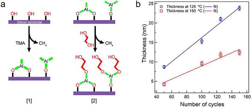
We have recently shown that nanopore zero-mode waveguides are effective tools for capturing picogram levels of long DNA fragments for single-molecule DNA sequencing. Despite these key advantages, the manufacturing of large arrays is not practical due to the need for serial nanopore fabrication. To overcome this challenge, we have developed an approach for the wafer-scale fabrication of waveguide arrays on low-cost porous membranes, which are deposited using molecular-layer deposition. The membrane at each waveguide base contains a network of serpentine pores that allows for efficient electrophoretic DNA capture at picogram levels while eliminating the need for prohibitive serial pore milling. Here, we show that the loading efficiency of these porous waveguides is up to 2 orders of magnitude greater than their nanopore predecessors. This new device facilitates the scaling-up of the process, greatly reducing the cost and effort of manufacturing. Furthermore, the porous zero-mode waveguides can be used for applications that benefit from low-input single-molecule real-time sequencing.

Keywords: Nanopore; SMRT sequencing; ZMWs; nanofabrication; porous membrane.


Figures

Figure 1.
Figure 1.
Porous membranes for electrokinetic biomolecular capture. (a) Illustration of the surface chemistry of molecular layer deposition (MLD) using trimethylaluminum (TMA) and ethylene glycol (EG). TMA is deposited on the native hydroxy surface of silicon nitride releasing CH4 as a byproduct [1], further exposing the surface to EG releasing CH4 as a byproduct, leaving the surface covered with hydroxylated groups [2]. (b) Thickness measurement of the hybrid organic–inorganic thin film using an ellipsometer as a function of a number of cycles for the same deposition temperature (error bars represent 1 standard deviation from 8 different samples deposited individually).
Figure 2.
Figure 2.
Neutron reflectivity of alucone on silicon. (a) Neutron reflectivity of alucone in buffers based on D2O, H2O, and a 2:1 mixture of D2O/H2O. Reflectivity is multiplied by Qz4, successive curves are offset by a factor of 10,2 and error bars are shown sparsely for clarity. Error bars represent 68% confidence intervals arising from Poisson counting uncertainty. (b) Residuals of volume occupancy model optimization to reflectivity curves. (c) SLD profiles of the alucone layer derived from the optimized volume occupancy model. Dashed lines are 95% confidence intervals. (d) The optimized underlying volume-occupancy model, showing good agreement with a free-form model (green curve; dashed lines are 95% confidence intervals or CI).
Figure 3.
Figure 3.
Experimental setup and DNA capture. (a) A Schematic of porous membrane on a free-standing SiN chip. The porous layer is deposited on top of the silicon nitride membrane, and back-etching the nitride exposes the thin porous region (shown as I and II). SiO2 is deposited atop porous layer using ALD technique for better surface chemistry, low noise, and low background signal. (b) Photoluminescence spectrum of the porous layer before and after nitride thinning. (c) A porous thin-region chip mounted on a fluorescence microscope with an integrated Faraday cage and patch clamp amplifier and reimaged via a 60×, 1.2 NA water immersion objective. (d) The IV curve of the porous thin-region membrane in 10 mM KCl (error bars represent one standard deviation from 5 measurements). (e) The kymograph shows a time series of DNA capture in two thin regions (shown as I and II); red and green boxes show the area of interest. Images are projections of all frames before (ON) and after (OFF) the application of voltage during an experiment and are both of the same fluorescence-intensity scale. Fluorescence intensity traces from two different porous thin regions (red and green rectangles) is seen when a voltage is applied (ON). In the absence (OFF) of bias, DNA is not captured, and no fluorescence activity is observed.
Figure 4.
Figure 4.
DNA loading using PZMW. (a) Scheme of the PZMW chip before and after etching silicon nitride. (b) Schematic representation of DNA loading on the cis side of the PZMW chip and applying a voltage bias. The panels represents an array of PZMWs in the same device during DNA loading at positive voltage bias. (c, d) An entire PZMW membrane (21 × 8 array), the image is a projection of all frames before applying voltage bias (0 mV). Red, green, and blue boxes show the area of interest for different PZMWs. The YOYO–DNAs were excited using 488 nm laser (5 mW laser power at objective plane, 60× water immersion), and the fluorescence traces from these PZMWs were recorded using emCCD over time are shown. In the absence of electric field, YOYO-I stained dsDNA are not captured (red and green traces), but over time, due to diffusion or voltage offset, DNA are seen to be captured (blue trace). (e, f) In the presence of applied voltage bias (70 mV), DNAs are immobilized in all of the PZMWs and is confirmed by the increase in the fluorescence intensity followed by photobleaching over time, captured using a emCCD camera and 60× objective lens. The intensity trace shows the activity of DNA capture in marked PZMWs. (g) IV curves of the a PZMW chip in 10 mM KCl before and after the experiment is shown (error bars represent 1 standard deviation from 10 measurements). (h) The capture rate of varying length of YOYO–DNA into PZMWs at 200 mV is plotted in units of millivolts per picomoles per minute (error bars represent 1 standard deviation) and is compared against the previously reported NZMW data at V = 200 mV (error bars are 1 standard deviation).

Similar articles

Cited by

References

    1. Sanger F; Nicklen S; Coulson AR Proc. Natl. Acad. Sci. U. S. A 1977, 74, 5463–7. - PMC - PubMed
    1. Rothberg JM; Leamon JH Nat. Biotechnol 2008, 26, 1117–24. - PubMed
    1. Eid J; Fehr A; Gray J; Luong K; Lyle J; Otto G; Peluso P; Rank D; Baybayan P; Bettman B; Bibillo A; Bjornson K; Chaudhuri B; Christians F; Cicero R; Clark S; Dalal R; Dewinter A; Dixon J; Foquet M; Gaertner A; Hardenbol P; Heiner C; Hester K; Holden D; Kearns G; Kong X; Kuse R; Lacroix Y; Lin S; Lundquist P; Ma C; Marks P; Maxham M; Murphy D; Park I; Pham T; Phillips M; Roy J; Sebra R; Shen G; Sorenson J; Tomaney A; Travers K; Trulson M; Vieceli J; Wegener J; Wu D; Yang A; Zaccarin D; Zhao P; Zhong F; Korlach J; Turner S Science 2009, 323, 133–8. - PubMed
    1. Levy SE; Myers RM Annu. Rev. Genomics Hum. Genet 2016, 17, 95–115. - PubMed
    1. Zhou B; Donnelly ME; Scholes DT; St George K; Hatta M; Kawaoka Y; Wentworth DE J. Virol 2009, 83, 10309. - PMC - PubMed

Publication types