

Infiltrated Photonic Crystal Fibers for Sensing Applications
- PMID: 30518084
- PMCID: PMC6308598
- DOI: 10.3390/s18124263
Infiltrated Photonic Crystal Fibers for Sensing Applications
Abstract
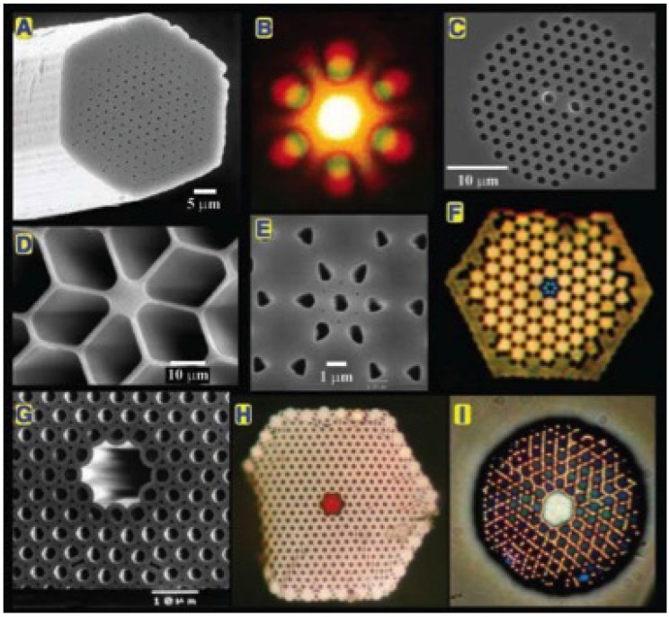
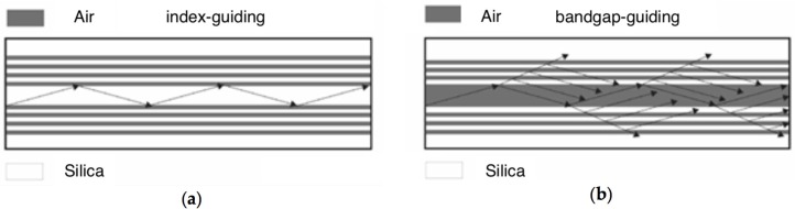
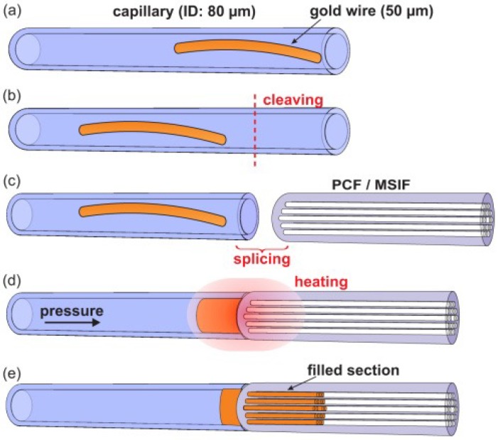
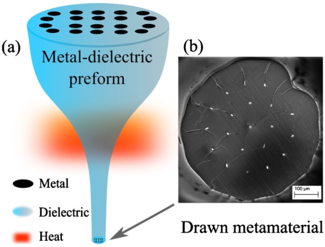
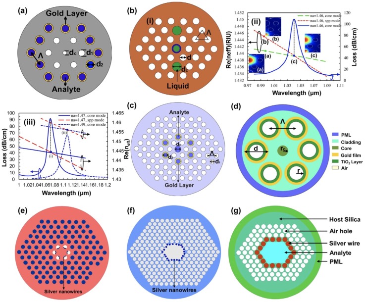
Photonic crystal fibers (PCFs) are a special class of optical fibers with a periodic arrangement of microstructured holes located in the fiber's cladding. Light confinement is achieved by means of either index-guiding, or the photonic bandgap effect in a low-index core. Ever since PCFs were first demonstrated in 1995, their special characteristics, such as potentially high birefringence, very small or high nonlinearity, low propagation losses, and controllable dispersion parameters, have rendered them unique for many applications, such as sensors, high-power pulse transmission, and biomedical studies. When the holes of PCFs are filled with solids, liquids or gases, unprecedented opportunities for applications emerge. These include, but are not limited in, supercontinuum generation, propulsion of atoms through a hollow fiber core, fiber-loaded Bose⁻Einstein condensates, as well as enhanced sensing and measurement devices. For this reason, infiltrated PCF have been the focus of intensive research in recent years. In this review, the fundamentals and fabrication of PCF infiltrated with different materials are discussed. In addition, potential applications of infiltrated PCF sensors are reviewed, identifying the challenges and limitations to scale up and commercialize this novel technology.
Keywords: liquid crystals; optical fiber sensors; optofluidics; photonic crystal fibers; plasmonic sensors.
Conflict of interest statement
The authors declare no conflict of interest.
Figures
Similar articles
-
Optical devices based on liquid crystal photonic bandgap fibres.Opt Express. 2003 Oct 6;11(20):2589-96. doi: 10.1364/oe.11.002589. Opt Express. 2003. PMID: 19471372
-
Hollow-Core Photonic Crystal Fiber Gas Sensing.Sensors (Basel). 2020 May 25;20(10):2996. doi: 10.3390/s20102996. Sensors (Basel). 2020. PMID: 32466269 Free PMC article. Review.
-
Photonic crystal fibers confining light by both index-guiding and bandgap-guiding: hybrid PCFs.Opt Express. 2007 Nov 26;15(24):15637-47. doi: 10.1364/oe.15.015637. Opt Express. 2007. PMID: 19550851
-
Prospects of Photonic Crystal Fiber as Physical Sensor: An Overview.Sensors (Basel). 2019 Jan 23;19(3):464. doi: 10.3390/s19030464. Sensors (Basel). 2019. PMID: 30678109 Free PMC article. Review.
-
Design and numerical analysis of a modified core hexa-deca photonic crystal fiber for highly negative dispersion and birefringence control in optical communication bands.Sci Rep. 2024 Nov 23;14(1):29075. doi: 10.1038/s41598-024-80539-3. Sci Rep. 2024. PMID: 39580537 Free PMC article.
Cited by
-
2D Au Nanosphere Arrays/PVA-PBA-Modified-Hydrogel Composite Film for Glucose Detection with Strong Diffraction Intensity and Linear Response.Nanomaterials (Basel). 2019 Jan 22;9(2):140. doi: 10.3390/nano9020140. Nanomaterials (Basel). 2019. PMID: 30678287 Free PMC article.
-
Optical Amplification in Hollow-Core Negative-Curvature Fibers Doped with Perovskite CsPbBr3 Nanocrystals.Nanomaterials (Basel). 2019 Jun 7;9(6):868. doi: 10.3390/nano9060868. Nanomaterials (Basel). 2019. PMID: 31181630 Free PMC article.
-
Fiber-Optic Temperature Sensor Using Cholesteric Liquid Crystals on the Optical Fiber Ferrules.Sensors (Basel). 2022 Aug 1;22(15):5752. doi: 10.3390/s22155752. Sensors (Basel). 2022. PMID: 35957311 Free PMC article.
-
Optical Fibre-Based Sensors for Oil and Gas Applications.Sensors (Basel). 2021 Sep 9;21(18):6047. doi: 10.3390/s21186047. Sensors (Basel). 2021. PMID: 34577252 Free PMC article. Review.
-
Review of Optical Fiber Sensors for Temperature, Salinity, and Pressure Sensing and Measurement in Seawater.Sensors (Basel). 2022 Jul 18;22(14):5363. doi: 10.3390/s22145363. Sensors (Basel). 2022. PMID: 35891043 Free PMC article. Review.
References
-
- Kashyap R., Wyatt R., McKee P.F. Wavelength flattened saturated erbium amplifier using multiple side-tap Bragg gratings. Electron. Lett. 1993;29:1025–1026. doi: 10.1049/el:19930685. - DOI
-
- Shigehara M., Satoh T., Inoue A., Hattori Y. Optical fiber identification system using fiber Bragg gratings. Opt. Fiber Commun. 1996:162–163.
-
- Udd E. An overview of fiber-optic sensors. Rev. Sci. Instrum. 1995;66:4015–4030. doi: 10.1063/1.1145411. - DOI
Publication types
Grants and funding
LinkOut - more resources
Full Text Sources
Other Literature Sources
