. 2018 Dec 5;9(1):5190.
doi: 10.1038/s41467-018-07508-z.

Plasmon induced thermoelectric effect in graphene

Affiliations

Plasmon induced thermoelectric effect in graphene

Viktoryia Shautsova et al. Nat Commun. .

Abstract

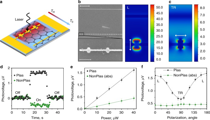
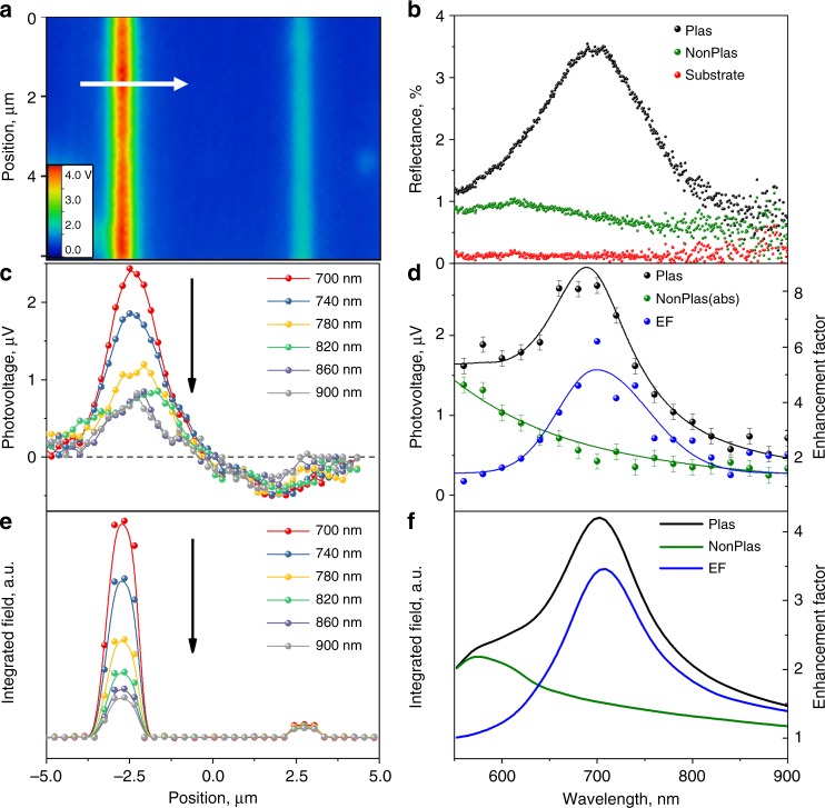
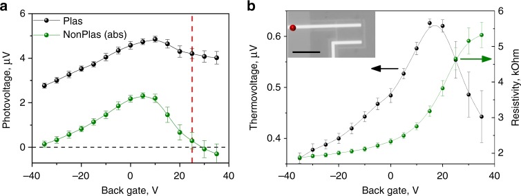
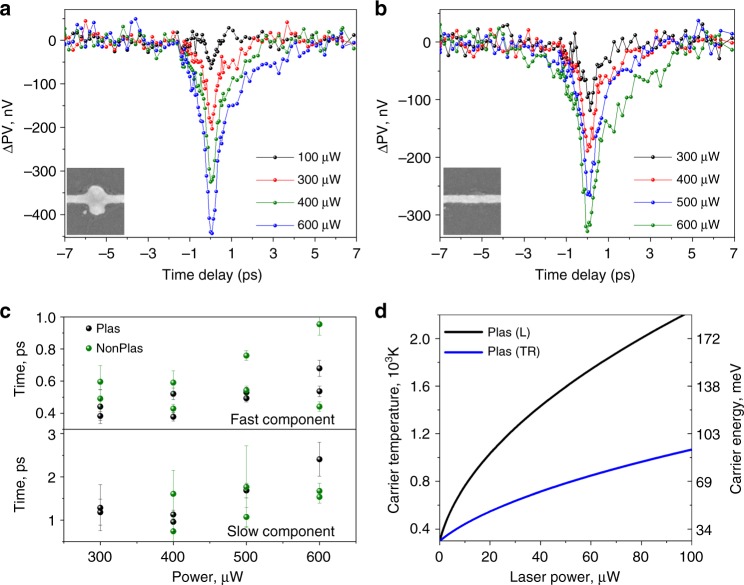
Graphene has emerged as a promising material for optoelectronics due to its potential for ultrafast and broad-band photodetection. The photoresponse of graphene junctions is characterized by two competing photocurrent generation mechanisms: a conventional photovoltaic effect and a more dominant hot-carrier-assisted photothermoelectric (PTE) effect. The PTE effect is understood to rely on variations in the Seebeck coefficient through the graphene doping profile. A second PTE effect can occur across a homogeneous graphene channel in the presence of an electronic temperature gradient. Here, we study the latter effect facilitated by strongly localised plasmonic heating of graphene carriers in the presence of nanostructured electrical contacts resulting in electronic temperatures of the order of 2000 K. At certain conditions, the plasmon-induced PTE photocurrent contribution can be isolated. In this regime, the device effectively operates as a sensitive electronic thermometer and as such represents an enabling technology for development of hot carrier based plasmonic devices.


Conflict of interest statement

The authors declare no competing interests.

Figures

Fig. 1
Fig. 1
Photocurrent generation mechanisms at graphene/metal interface. a Schematic of a graphene/Au interface and associated band diagrams for various gating conditions. The black dash line represents the Fermi level and the black dotted line represents the Dirac point of the graphene. The illumination is localized at the graphene/Au interface resulting in a higher local carrier temperature (TH) compared to the bath temperature (T0). b Calculated gate voltage dependence of Fermi level difference (top) and Seebeck coefficient difference (middle) between the Gr/Au and Gr/SiO2 areas and gate voltage dependence of Seebeck coefficient for the graphene channel (bottom). The contributing current directions are indicated by arrows. Vertical red (dash) and black (dash–dot) lines correspond to the flat band and Dirac points, respectively. Seebeck coefficients are calculated based on the conductivity model at T = 300 K. See Supplementary Discussion 1 for the calculation details
Fig. 2
Fig. 2
Photoresponse of a metal–graphene–metal photodetector with asymmetric plasmonic contacts. a Schematic of the graphene device with plasmonic and nonplasmonic contacts. Under optical excitation of the plasmonic contact, the local electronic temperature rises to TH compared to the bath temperature (T0) resulting in the temperature gradient established across the contacts as indicated by the arrow. b Scanning electron microscopic image of the device (upper panel, scale bar is 2 µm) and graphene/Au nanostructures (lower panel, scale bar is 300 nm). c Calculated electromagnetic field distributions for longitudinal (L) and transverse (TR) polarization at 740 nm. df Photovoltage generated at 740 nm as a function of time (d), laser power (e) and polarization (f) for plasmonic (Plas) and nonplasmonic (NonPlas) contacts. For ease of comparison, the photovoltage generated for the nonplasmonic contact is presented in absolute values (abs). The measurements in d, e were performed under L polarization. The laser power in d, f is fixed at 40 µW. The error bars are the standard deviation in the measurements
Fig. 3
Fig. 3
Plasmon-enhanced graphene photoresponse. a Dark field microscopic image of the graphene device with plasmonic (left) and nonplasmonic contacts (right). b Corresponding dark field reflection spectra. c Photovoltage line scans across the device in the direction indicated by the arrow in a taken at different excitation wavelengths. d Wavelength dependence of the photovoltage (absolute value) from the plasmonic and nonplasmonic contacts. Enhancement factor is determined as following VPlas/VNonPlas. The photovoltage measurements are performed with an elliptical laser spot with 40 µW power. e Calculated line scan of the integrated electromagnetic field. f Calculated wavelength dependence of the integrated electromagnetic field and enhancement factor (Plas/NonPlas). The error bars are the standard deviation in the measurements
Fig. 4
Fig. 4
Gate-dependent photovoltage and thermoelectric response. a The photovoltage response of plasmonic and nonplasmonic (absolute value) contacts. Photovoltage measurements are performed with an elliptical laser spot at 700 nm with 40 µW power under longitudinal polarization. The vertical dash line represents the flat-band condition. It should be noted that a direct comparison of the photovoltage generated for the plasmonic and nonplasmonic contacts in terms of absolute values is complicated owing to contact imperfections (Supplementary Discussion 3). b The thermoelectric voltage and square resistance of a representative FET device. Inset: greyscale optical microscopic image of the device with the laser position marked by a red dot. Scale bar is 10 µm. Measurements are performed with a focussed laser spot at 750 nm and 3 mW power. The error bars are the standard deviation in the measurements
Fig. 5
Fig. 5
Plasmon-induced carrier heating. a, b Probe-induced photovoltage at plasmonic and nonplasmonic contacts as a function of pump–probe pulse delay time. Probe at wavelength of 750 nm and 100 µW power, pump at a wavelength of 650 nm and power as indicated; both beam spots have elliptical shape. c Response time extracted from the bi-exponential decay of the dip in a, b as a function of the pump power. Error bars reflect the estimated standard deviation of the fit coefficients. d Power dependence of the carrier temperature and carrier energy in graphene at the plasmonic contact under longitudinal (L) and transverse (TR) polarizations

References

    1. Gabor NM, et al. Hot carrier-assisted intrinsic photoresponse in graphene. Science. 2011;334:648–652. doi: 10.1126/science.1211384. - DOI - PubMed
    1. Liu CH, Dissanayake NM, Lee S, Lee K, Zhong Z. Evidence for extraction of photoexcited hot carriers from graphene. ACS Nano. 2012;6:7172–7176. doi: 10.1021/nn302227r. - DOI - PubMed
    1. Song JCW, Rudner MS, Marcus CM, Levitov LS. Hot carrier transport and photocurrent response in graphene. Nano Lett. 2011;11:4688–4692. doi: 10.1021/nl202318u. - DOI - PubMed
    1. Xu X, Gabor NM, Alden JS, van der Zande AM, McEuen PL. Photo-thermoelectric effect at a graphene interface junction. Nano Lett. 2010;10:562–566. doi: 10.1021/nl903451y. - DOI - PubMed
    1. Lemme MC, et al. Gate-activated photoresponse in a graphene p-n junction. Nano Lett. 2011;11:4134–4137. doi: 10.1021/nl2019068. - DOI - PubMed

Publication types