. 2018 Dec 17;9(1):5354.
doi: 10.1038/s41467-018-07706-9.

Single crystal hybrid perovskite field-effect transistors

Affiliations

Single crystal hybrid perovskite field-effect transistors

Weili Yu et al. Nat Commun. .

Abstract

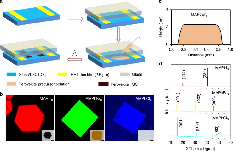
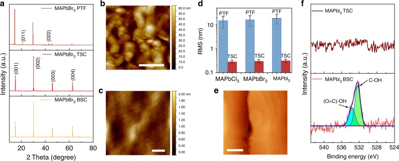
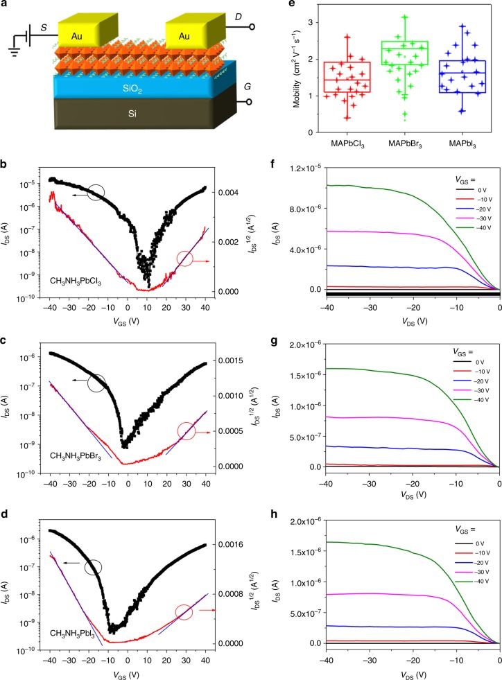
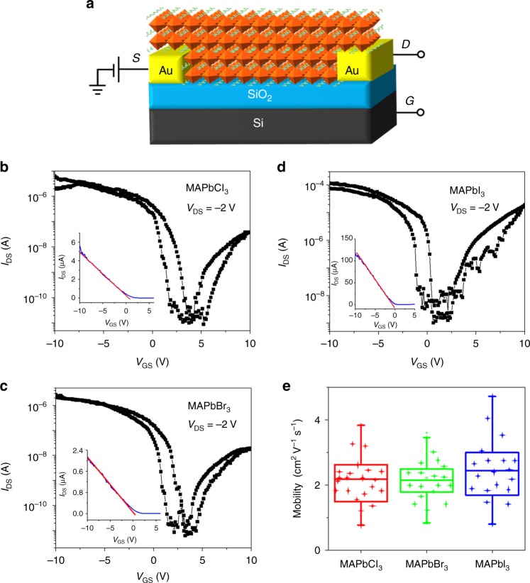
The fields of photovoltaics, photodetection and light emission have seen tremendous activity in recent years with the advent of hybrid organic-inorganic perovskites. Yet, there have been far fewer reports of perovskite-based field-effect transistors. The lateral and interfacial transport requirements of transistors make them particularly vulnerable to surface contamination and defects rife in polycrystalline films and bulk single crystals. Here, we demonstrate a spatially-confined inverse temperature crystallization strategy which synthesizes micrometre-thin single crystals of methylammonium lead halide perovskites MAPbX3 (X = Cl, Br, I) with sub-nanometer surface roughness and very low surface contamination. These benefit the integration of MAPbX3 crystals into ambipolar transistors and yield record, room-temperature field-effect mobility up to 4.7 and 1.5 cm2 V-1 s-1 in p and n channel devices respectively, with 104 to 105 on-off ratio and low turn-on voltages. This work paves the way for integrating hybrid perovskite crystals into printed, flexible and transparent electronics.


Conflict of interest statement

W.Y., A.A., and L.Y. have a US patent application related to this work (Filed on 10 June 2016, WO2018047066). The remaining authors declare no competing interests.

Figures

Fig. 1
Fig. 1
Hybrid perovskite TSC fabrication. a Schematic representation of spatially confined inverse temperature crystallization method for producing thin single crystals (TSCs). b Fluorescence microscopy images of MAPbI3, MAPbBr3, and MAPbCl3 TSCs (which are excited with a pulsed 450, 473, and 405 nm laser, respectively). Scale bar: 100 μm. Inset: optical images of MAPbI3, MAPbBr3, and MAPbCl3 TSCs. Scale bar: 200 μm. c Height profile of MAPbBr3 TSC indicating its thickness is about 2.45 µm. d XRD spectra of synthesized MAPbX3 TSCs, where X = I, Br, and Cl, respectively
Fig. 2
Fig. 2
Microstructure and surface properties of TSCs. a XRD data comparing the polycrystalline thin film (PTF) to the TSC and bulk single crystal (BSC) forms of MAPbBr3. Surface topography of a MAPbBr3 PTF (b) and that of a TSC (c) as measured by AFM, of which the root mean squared (RMS) roughness for PTF and TSC are 16.5 and 0.21 nm, respectively. Scale bar: 400 nm. d RMS surface roughness of MAPbX3 (X = Cl, Br, and I) polycrystalline film and TSCs. The error bar reflects the statistical variation in roughness in different parts of the sample. e Scanning tunneling microscopy (STM) image of the surface region near the edge of a MAPbBr3 TSC. Scale bar: 50 nm. f XPS spectra of the surface of MAPbI3 TSC and BSC
Fig. 3
Fig. 3
Characteristics of top-contact TSC-FETs. a Schematic of the bottom-gate, top-contact (BGTC) device with a TSC hybrid perovskite as semiconductor layer. Transfer characteristics (IDS vs. VGS (black solid square) and IDS1/2 vs. VGS (red solid line)), as well as the fit lines (blue solid line) for b MAPbCl3, c MAPbBr3, and d MAPbI3 TSC-FETs, VGS ranging from −40 to 40 V. VDS = −30 V. e Saturation mobility statistics for 60 devices. The box plot graphically depicts the statistical population of numerical data, including the maximum, the minimum, as well as the average (median) mobilities. Channel length: 50 μm. Output characteristics of TSC-FETs based on f MAPbCl3, g MAPbBr3, and h MAPbI3
Fig. 4
Fig. 4
Characteristics of bottom-contact TSC-FETs. a Schematic representation of bottom-gate, bottom-contact (BGBC) TSC-FET device. Representative transfer characteristics of TSC-FETs of b MAPbCl3, c MAPbBr3, and d MAPbI3 using forward/reverse gate voltage sweeps from −10 to 10 V at a rate of 0.05 V s−1, with VDS = −2 V. Insets of bd show the linear regime of the respective devices. e Field-effect hole mobility distribution for 20 devices fabricated and tested for each halide perovskite

References

    1. Kojima A, Teshima K, Shirai Y, Miyasaka T. Organometal halide perovskites as visible-light sensitizers for photovoltaic cells. J. Am. Chem. Soc. 2009;131:6050–6051. doi: 10.1021/ja809598r. - DOI - PubMed
    1. Lee MM, Teuscher J, Miyasaka T, Murakami TN, Snaith HJ. Efficient hybrid solar cells based on meso-superstructured organometal halide perovskites. Science. 2012;338:643–647. doi: 10.1126/science.1228604. - DOI - PubMed
    1. Yang WS, et al. High-performance photovoltaic perovskite layers fabricated through intramolecular exchange. Science. 2015;348:1234–1237. doi: 10.1126/science.aaa9272. - DOI - PubMed
    1. Guo YL, Yu G, Liu YQ. Functional organic field-effect transistors. Adv. Mater. 2010;22:4427–4447. doi: 10.1002/adma.201000740. - DOI - PubMed
    1. Wang CL, Dong HL, Hu WP, Liu YQ, Zhu DB. Semiconducting pi-conjugated systems in field-effect transistors: a material odyssey of organic electronics. Chem. Rev. 2012;112:2208–2267. doi: 10.1021/cr100380z. - DOI - PubMed

Publication types