. 2019 Jan 3;10(1):54.
doi: 10.1038/s41467-018-07904-5.

Three-dimensional monolithic integration in flexible printed organic transistors

Affiliations

Three-dimensional monolithic integration in flexible printed organic transistors

Jimin Kwon et al. Nat Commun. .

Abstract

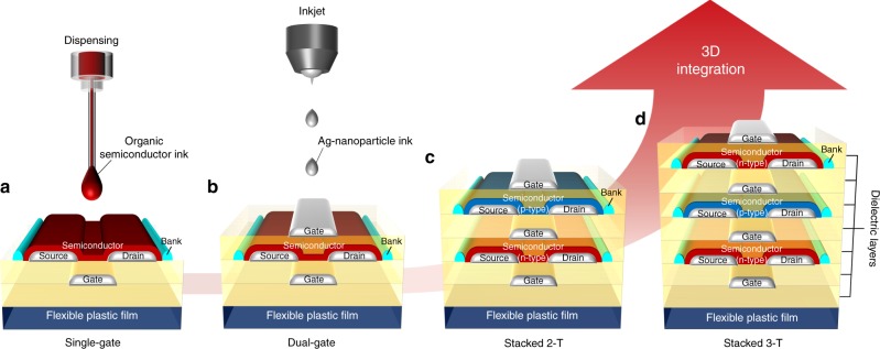
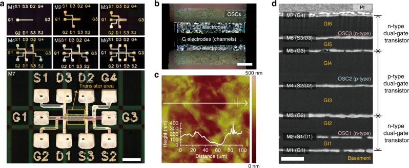
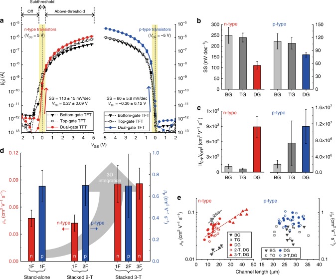
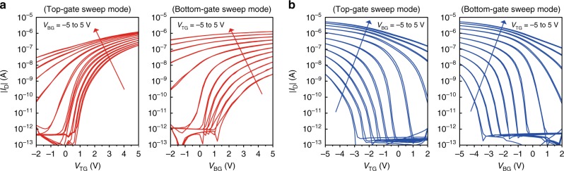
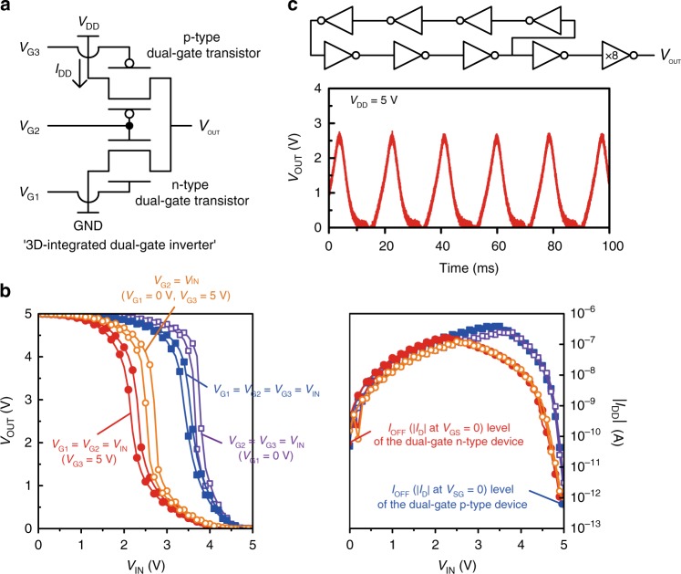
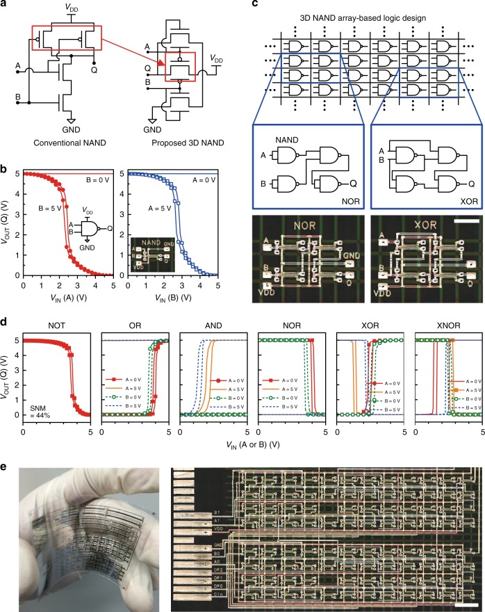
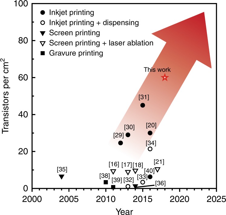
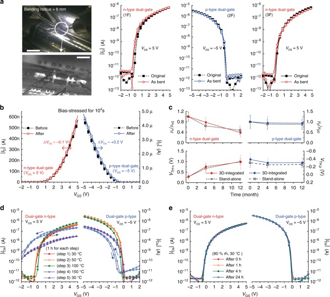
Direct printing of thin-film transistors has enormous potential for ubiquitous and lightweight wearable electronic applications. However, advances in printed integrated circuits remain very rare. Here we present a three-dimensional (3D) integration approach to achieve technology scaling in printed transistor density, analogous to Moore's law driven by lithography, as well as enhancing device performance. To provide a proof of principle for the approach, we demonstrate the scalable 3D integration of dual-gate organic transistors on plastic foil by printing with high yield, uniformity, and year-long stability. In addition, the 3D stacking of three complementary transistors enables us to propose a programmable 3D logic array as a new route to design printed flexible digital circuitry essential for the emerging applications. The 3D monolithic integration strategy demonstrated here is applicable to other emerging printable materials, such as carbon nanotubes, oxide semiconductors and 2D semiconducting materials.


Conflict of interest statement

The authors declare no competing interests.

Figures

Fig. 1
Fig. 1
3D monolithic integration in flexible printed transistors. a, b Printed single-gate and dual-gate organic transistors. c, d 3D-integrated two (n-/p-type, stacked 2-T) and three (n-/p-/n-type, stacked 3-T) complementary dual-gate organic transistors with shared gate electrodes. All the films were printed except for the Parylene dielectric layers
Fig. 2
Fig. 2
Images of a stacked 3-T device. a Sequential images of the process of printing seven metal layers (scale bar is 1 mm). b A polarized microscopy image of the transistor area (scale bar is 200 μm). c A topographic AFM image (scan area is 100 × 100 μm) measured on top of the channel area. The inset graph shows the profile along the cross-section line. d Cross-sectional SEM image of the stacked 3-T device (M1-7: metal layers, GI1-6: dielectric insulator layers, OSC1-3: organic semiconductor layers, scale bar is 250 nm, Pt was sputtered on the top prior to the SEM measurement)
Fig. 3
Fig. 3
Device characteristics. a |ID|–VGS transfer characteristics of the n-type and p-type organic transistors in single-gate (bottom-gate and top-gate) and dual-gate configurations. b The subthreshold swings and c the ID on-off ratios. d The extracted carrier mobilities in the 3D-integrated complementary organic transistors. e The channel length dependency of the extracted carrier mobilities. Error bars represent standard deviation
Fig. 4
Fig. 4
Dual-gate complementary transistor operations. a Saturation transfer characteristics (VDS = 5 V) of the n-type dual-gate transistor in top-gate (left) and bottom-gate (right) sweeping modes (VTG: top-gate voltage, VBG: bottom-gate voltage). b Saturation transfer characteristics (VDS = −5 V) of the p-type dual-gate transistor in top-gate (left) and bottom-gate (right) modes
Fig. 5
Fig. 5
Stacked 2-T dual-gate devices. a Schematic circuit of the 3D-integrated dual-gate inverter (VG1, VG2, VG3: gate inputs, IDD: static current from the source). b Voltage transfer characteristics (left) and static currents (right) of the inverter operation according to the combinations of electrical gate connections. c Schematic circuit of the ring oscillator which is composed of seven 3D-integrated dual-gate inverters and its oscillation operation. The buffer output stage consists of serially connected two inverters, where the transistor W of the last inverter is designed to be eight times larger than that of the others
Fig. 6
Fig. 6
3D NAND digital circuit design based on stacked 3-T dual-gate devices. a Schematic circuits of a conventional NAND gate and a proposed 3D NAND gate. b DC VOUTVIN characteristics of a 3D NAND gate. c 3D NAND array-based logic design (scale bar is 2 mm). d DC VINVOUT characteristics of a 1-input NOT gate and 2-input (A and B) logic gates (OR, AND, NOR, XOR, and XNOR) implemented by interconnecting 3D NANDs. A fixed voltage (0 or 5 V) is applied to one port while a voltage input on the other port is swept. e A large-scale flexible logic circuitry implemented by using a 12 × 8 3D NAND gate array (scale bar is 4 mm)
Fig. 7
Fig. 7
Transistor density trend of printed organic circuits fabricated by various printing techniques
Fig. 8
Fig. 8
Mechanical, electrical, long-term, and environmental reliabilities a Images of the stacked 3-T device under bending test (white dotted area is magnified) and its saturation transfer characteristics as bent on a curved surface (scale bars in the top and bottom images are 1 cm and 1 mm, respectively). b Shift of the saturation transfer characteristics of the printed stand-alone complementary transistors after electrical bias stress for 10,000 s (at VGS = VDS = 5 V for the n-type and −5 V for the p-type). c Year-long observation on the carrier mobilities and threshold voltages of the stand-alone and stacked 2-T devices (μn, μp: carrier mobility, μn0, μp0: initial carrier mobility, VTH,n, VTH,p: threshold voltage, error bars represent standard deviation). d Shift of the saturation transfer characteristics of the complementary dual-gate transistors under consecutive five thermal stress steps. e Shift of the saturation transfer characteristics of the complementary dual-gate transistors under a humid environment (90% rh, 30 °C) for 24 h (rh: relative humidity)

References

    1. Wang S, et al. Skin electronics from scalable fabrication of an intrinsically stretchable transistor array. Nature. 2018;555:83–88. doi: 10.1038/nature25494. - DOI - PubMed
    1. Baeg KJ, Caironi M, Noh YY. Toward printed integrated circuits based on unipolar or ambipolar polymer semiconductors. Adv. Mater. 2013;25:4210–4244. doi: 10.1002/adma.201205361. - DOI - PubMed
    1. Kang B, Lee WH, Cho K. Recent advances in organic transistor printing processes. ACS Appl. Mater. Interfaces. 2013;5:2302–2315. doi: 10.1021/am302796z. - DOI - PubMed
    1. Lim JA, Lee HS, Lee WH, Cho K. Control of the morphology and structural development of solution-processed functionalized acenes for high-performance organic transistors. Adv. Funct. Mater. 2009;19:1515–1525. doi: 10.1002/adfm.200801135. - DOI
    1. Torrisi F, et al. Inkjet-printed graphene electronics. ACS Nano. 2012;6:2992–3006. doi: 10.1021/nn2044609. - DOI - PubMed

Publication types