. 2019 Jan 4;5(1):eaat1451.
doi: 10.1126/sciadv.aat1451. eCollection 2019 Jan.

Nonlinear integrated quantum electro-optic circuits

Affiliations

Nonlinear integrated quantum electro-optic circuits

Kai-Hong Luo et al. Sci Adv. .

Abstract

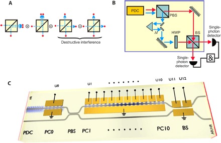
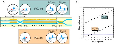
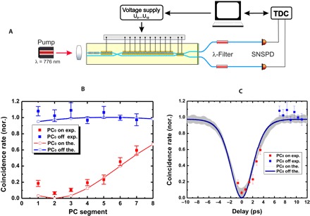
Future quantum computation and networks require scalable monolithic circuits, which incorporate various advanced functionalities on a single physical substrate. Although substantial progress for various applications has already been demonstrated on different platforms, the range of diversified manipulation of photonic states on demand on a single chip has remained limited, especially dynamic time management. Here, we demonstrate an electro-optic device, including photon pair generation, propagation, electro-optical path routing, as well as a voltage-controllable time delay of up to ~12 ps on a single Ti:LiNbO3 waveguide chip. As an example, we demonstrate Hong-Ou-Mandel interference with a visibility of more than 93 ± 1.8%. Our chip not only enables the deliberate manipulation of photonic states by rotating the polarization but also provides precise time control. Our experiment reveals that we have full flexible control over single-qubit operations by harnessing the complete potential of fast on-chip electro-optic modulation.


Figures

Fig. 1
Fig. 1. A miniaturized compact quantum circuit with active and accurate manipulation in LiNbO3 waveguides.
(A) HOM bunching effect of indistinguishable photons in a BS. (B) Schematics of a typical HOM experiment using bulk optic components. Photon pairs with orthogonal polarizations and degenerate frequencies are generated via type II phase-matched PDC. A PBS is used to spatially separate the photons. To produce two identical photons, one photon is delayed in time, and its polarization is rotated by a half-wave plate (HWP) with respect to the other one. The photons are recombined again on a BS. All the functionalities in the yellow box are integrated into the chip. (C) Scheme of the integrated quantum optical chip with monolithically integrated PDC source, electro-optic PCs, PBS, and BS. The gray lines denote the Ti-indiffused waveguides. In the periodically poled PDC section, orthogonally polarized photon pairs (H and V) are generated. In the subsequent PC0, the complete conversion changes the polarization state of both photons from H to V and vice versa via applying the control voltages U0. These photons are spatially separated by the PBS. The H-polarized photons leave the splitter at the bar-state output, and V photons leave the splitter at the cross-state output. The H photons (at the bar-state output of the splitter) enter into the segmented PC. At a certain position [depending on the voltages (U1 to U10) applied to the various segments], the polarization state is converted to V. Thus, these photons and the photons from the second branch enter the BS in V polarization. BS is realized as a directional coupler with Δβ reversal electrodes. A 50:50 splitting ratio is precisely adjusted via the two control voltages U11 and U12. The waveguide end-faces are with antireflection (AR) and high reflection (HR) coatings.
Fig. 2
Fig. 2. Illustration of the principle of the adjustable BED line.
(A) The diagram shows the chip design together with some insets illustrating the temporal relation of the horizontally (red) and vertically (blue) polarized photon wave packets at different positions of the structure and for various configurations of the PCs. Case I: If PC0 is switched off, then the temporal walk-off increases along the structure. Thus, the time delay between the two photons can be varied, depending on which element of the segmented converter is switched on; however, the two photons will never arrive simultaneously at the BS. Case II: If PC0 is switched on, then the originally horizontally polarized photon can overtake the other photon before they arrive at the segmented PC. A simultaneous arrival of the two photons at the BS can be achieved if a certain element of the segmented PC is addressed. (B) Calculated time delay of the photons at the BS as a function of the element of the segmented PC, at which the final swapping of the polarization is performed. The diagram shows the result for the two cases of PC0 on and off. The dotted line indicates the time synchronization between the two polarized photons. The parameters used for the calculations are adapted to the geometry of the fabricated device—lengths of the PDC section (20.7 mm), PC0 (7.62 mm), the PBS section (4.0 mm), and a single element of the segmented converters (2.54 mm). A group index difference Δng = 0.0805 has been derived from the Sellmeier equations of LiNbO3 (λ = 1551.7 nm).
Fig. 3
Fig. 3. Classical characterization of the integrated circuit.
(A) Normalized power of the second harmonic (SH) wave generated in the PDC section with a poling period of ΛPDC = 9.04 μm as a function of the fundamental wavelength, which is from a tunable telecom laser with narrow bandwidth. (B) Spectral transmission characteristics of PC0 and the various triple combinations of the segmented PC (with a poling period of ΛPC = 21.4 μm). We obtained the curves by launching broadband incoherent light in the telecom range and measuring the unconverted power behind a polarizer. The curves are normalized to a reference transmission spectrum obtained without conversion. (C) Temperature dependence of the two phase-matching processes (PDC and PC). The crossing of the two curves determines the optimum operation point, which is at T = 43.6°C and λ = 1551.7 nm.
Fig. 4
Fig. 4. Experimental setup and quantum results.
(A) Experimental setup for quantum characterization of the active HOM chip. A tunable narrowband continuous-wave pump laser around 776 nm is coupled into the channel with the PDC source. To avoid higher-order photon pair generation, the pump power is kept in the range of 100 μW. A temperature controller controls and stabilizes the previously determined temperature distribution of the sample. The two output ports from the chip are directly coupled into a pair of single-mode fibers. Via fiber-optical isolators to suppress the residual pump light and a 1.2-nm bandpass filter to suppress background photons, the transmitted photons are detected with superconducting nanowire detectors (SNSPDs) and time-to-digital converter (TDC). (B) Experimental and simulated results of the normalized coincidence rate as a function of which triple of the segmented PC is driven. The blue data and curve are for PC0 off, while the red data and curve are for PC0 on. In the experiment, only seven triples of the segmented PC could be addressed because the electrode of PC10 was broken. Therefore, only 14 different delays were possible. (C) Experimental and simulated profiles of the HOM dip derived from the coincidence results shown in (B) and the corresponding calculated time delay.

References

    1. Politi A., Cryan M. J., Rarity J. G., Yu S., O’Brien J. L., Silica-on-silicon waveguide quantum circuits. Science 320, 646–649 (2008). - PubMed
    1. Carolan J., Harrold C., Sparrow C., Martín-López E., Russell N. J., Silverstone J. W., Shadbolt P. J., Matsuda N., Oguma M., Itoh M., Marshall G. D., Thompson M. G., Matthews J. C. F., Hashimoto T., O’Brien J. L., Laing A., Universal linear optics. Science 349, 711–716 (2015). - PubMed
    1. Silverstone J. W., Bonneau D., Ohira K., Suzuki N., Yoshida H., Iizuka N., Ezaki M., Natarajan C. M., Tanner M. G., Hadfield R. H., Zwiller V., Marshall G. D., Rarity J. G., O’Brien J. L., Thompson M. G., On-chip quantum interference between silicon photon-pair sources. Nat. Photonics 8, 104–108 (2014).
    1. Giovannetti V., Lloyd S., Maccone L., Advances in quantum metrology. Nat. Photonics 5, 222–229 (2011).
    1. Tillmann M., Dakić B., Heilmann R., Nolte S., Szameit A., Walther P., Experimental boson sampling. Nat. Photonics 7, 540–544 (2013).