. 2019 Jan 14;10(1):180.
doi: 10.1038/s41467-018-08088-8.

Pseudodoping of a metallic two-dimensional material by the supporting substrate

Affiliations

Pseudodoping of a metallic two-dimensional material by the supporting substrate

Bin Shao et al. Nat Commun. .

Abstract

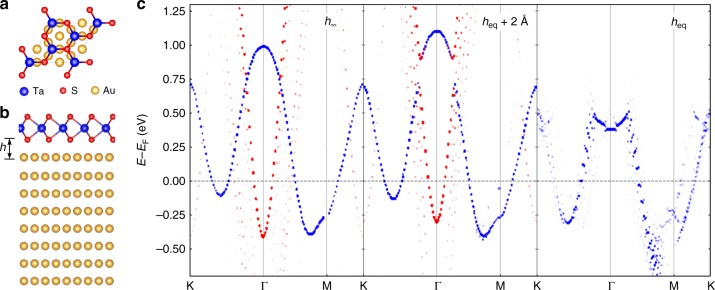
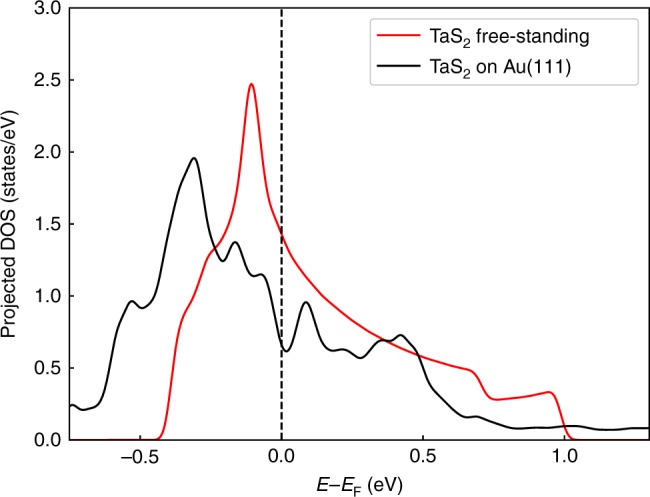
Charge transfers resulting from weak bondings between two-dimensional materials and the supporting substrates are often tacitly associated with their work function differences. In this context, two-dimensional materials could be normally doped at relatively low levels. Here, we demonstrate how even weak hybridization with substrates can lead to an apparent heavy doping, using the example of monolayer 1H-TaS2 grown on Au(111). Ab-initio calculations show that sizable changes in Fermi areas can arise, while the transferred charge between substrate and two-dimensional material is much smaller than the variation of Fermi areas suggests. This mechanism, which we refer to as pseudodoping, is associated with non-linear energy-dependent shifts of electronic spectra, which our scanning tunneling spectroscopy experiments reveal for clean and defective TaS2 monolayer on Au(111). The influence of pseudodoping on the formation of many-body states in two-dimensional metallic materials is analyzed, shedding light on utilizing pseudodoping to control electronic phase diagrams.


Conflict of interest statement

The authors declare no competing interests.

Figures

Fig. 1
Fig. 1
Pseudodoping of TaS2 on Au(111). Supercell of monolayer 1H-TaS2 on Au(111), a top view and b side view. The adsorption height h refers to the height of the lowest S atoms above the uppermost Au atoms. c Projection of upfolded band structures on Ta-d orbitals (blue dots) and upmost Au-pz orbitals (red dots) as a function of adsorption height: h, heq + 2 Å, and heq. The h case consists of two separated systems: a clean Au(111) substrate and a free-standing 1H-TaS2 monolayer
Fig. 2
Fig. 2
Scanning tunneling microscopy and spectroscopy of TaS2 on Au(111). a High-resolution STM topography in the constant-current mode, where the color bar is related to the measured apparent height and the length of the scalar bar is 5 nm, STM parameters: Sample bias voltage VS = 335 mV, tunneling current IT = 500 pA. b Comparison of STS point spectra from the sites with/without defects. STS parameters: Stabilization voltage Vstab = 1 V, stabilization current Istab = 500 pA, modulation voltage Vmod = 5 mV. The corresponding measurement sites are represented by the spots in a. c STS simulations as a function of the adsorption height h
Fig. 3
Fig. 3
Minimal two-band model of pseudodoping. Evolution of a the energy dispersion and b the orbital/band occupation NabN as a function of the hybridization (t) between the orbital |a〉 of 2d materials and |b〉 of substrates. As illustrated in a, the hybridization leads to an admixture of substrate derived states (red) to the 2d material states (blue) and a level repulsion between the hybridizing bands. The level repulsion, as t increases, allows the band occupation N to vary sizably, i.e., the upper band |+〉 (the lower band |−〉) is apparently doped by holes (electrons), while leaving the orbital occupation Na/b almost unchanged as shown in b. Ntot refers to the total occupation number of the system, which is a constant under the variation in t
Fig. 4
Fig. 4
Influence of the Au(111) substrate on the TaS2 DOS. Comparison of the DOS projected on Ta-d orbitals of 1H-TaS2 on Au(111) substrate (black line) and in its free-standing form (red line)

References

    1. Novoselov KS, et al. Two-dimensional atomic crystals. PNAS. 2005;102:10451–10453. doi: 10.1073/pnas.0502848102. - DOI - PMC - PubMed
    1. Novoselov KS, Mishchenko A, Carvalho A, Castro Neto AH. 2d materials and van der Waals heterostructures. Science. 2016;353:aac9439. doi: 10.1126/science.aac9439. - DOI - PubMed
    1. Miro P, Audiffred M, Heine T. An atlas of two-dimensional materials. Chem. Soc. Rev. 2014;43:6537–6554. doi: 10.1039/C4CS00102H. - DOI - PubMed
    1. Qing-Yan W, et al. Interface-induced high-temperature superconductivity in single unit-cell FeSe films on SrTiO3. Chin. Phys. Lett. 2012;29:037402. doi: 10.1088/0256-307X/29/3/037402. - DOI
    1. Ge JF, et al. Superconductivity above 100 K in single-layer FeSe films on doped SrTiO3. Nat. Mater. 2014;14:285–289. doi: 10.1038/nmat4153. - DOI - PubMed

Publication types