

Measurement and Evaluation of Local Surface Temperature Induced by Irradiation of Nanoscaled or Microscaled Electron Beams
- PMID: 30671671
- PMCID: PMC6342749
- DOI: 10.1186/s11671-018-2821-x
Measurement and Evaluation of Local Surface Temperature Induced by Irradiation of Nanoscaled or Microscaled Electron Beams
Abstract
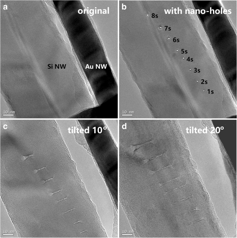
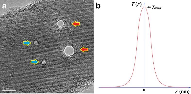
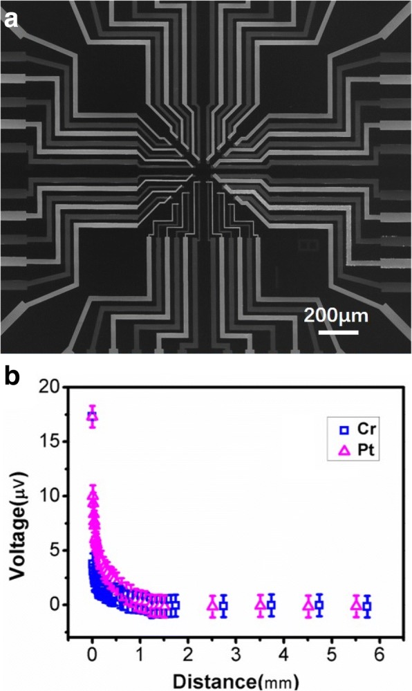
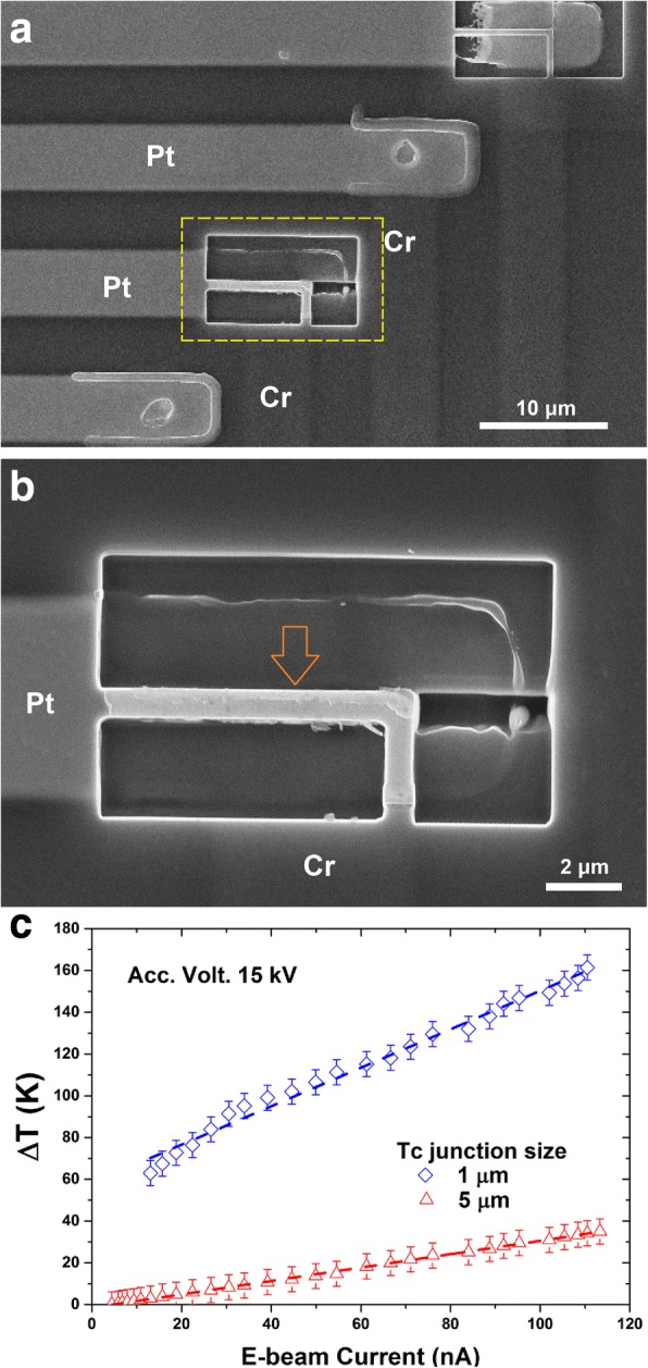
Electron beams (e-beams) have been applied as detecting probes and clean energy sources in many applications. In this work, we investigated several approaches for measurement and estimation of the range and distribution of local temperatures on a subject surface under irradiation of nano-microscale e-beams. We showed that a high-intensity e-beam with current density of 105-6 A/cm2 could result in vaporization of solid Si and Au materials in seconds, with a local surface temperature higher than 3000 K. With a lower beam intensity to 103-4 A/cm2, e-beams could introduce local surface temperature in the range of 1000-2000 K shortly, causing local melting in metallic nanowires and Cr, Pt, and Pd thin films, and phase transition in metallic Mg-B films. We demonstrated that thin film thermocouples on a freestanding Si3N4 window were capable of detecting peaked local surface temperatures up to 2000 K and stable, and temperatures in a lower range with a high precision. We discussed the distribution of surface temperatures under e-beams, thermal dissipation of thick substrate, and a small converting ratio from the high kinetic energy of e-beam to the surface heat. The results may offer some clues for novel applications of e-beams.
Keywords: Electron beam; Energy converting; Local temperature; Melting point; Nanoscale thermometry; Scanning electron microscopy; Thin film thermocouple; Transmission electron microscopy; Vaporization.
Conflict of interest statement
Competing Interests
The authors declare that they have no competing interests.
Publisher’s Note
Springer Nature remains neutral with regard to jurisdictional claims in published maps and institutional affiliations.
Figures


References
-
- Babin S. Measurement of resist heating in photomask fabrication. J Vac Sci Technol B. 1997;15:2209–2213. doi: 10.1116/1.589615. - DOI
-
- Babin S, Kahng AB, Măndoiu II, Muddu S. Improving critical dimension accuracy and throughput by subfield scheduling in electron beam mask writing. J Vac Sci Technol B. 2005;23:3094–3100. doi: 10.1116/1.2132330. - DOI
-
- Jugessur A, Yagnyukova M, Aitchison J. Nanofabrication of photonic crystal-based devices using electron beam spot lithography. J Vac Sci Technol B. 2011;29:06FF06. doi: 10.1116/1.3662088. - DOI
-
- Thin-film deposition . Principles and practice. New York: McGraw-hill; 1995.
-
- Dai Q, Kong XD, Feng QR, Yang QQ, Zhang H, Nie RJ, Han L, Ma YW, Wang FR. MgB2 films prepared by rapid annealing method. Physica C. 2012;475:24–27. doi: 10.1016/j.physc.2012.01.014. - DOI
Grants and funding
LinkOut - more resources
Full Text Sources
