Review
. 2018 Nov 1;9(11):565.
doi: 10.3390/mi9110565.

Oriented Carbon Nanostructures by Plasma Processing: Recent Advances and Future Challenges

Affiliations
Review

Oriented Carbon Nanostructures by Plasma Processing: Recent Advances and Future Challenges

Neelakandan M Santhosh et al. Micromachines (Basel). .

Abstract

Carbon, one of the most abundant materials, is very attractive for many applications because it exists in a variety of forms based on dimensions, such as zero-dimensional (0D), one-dimensional (1D), two-dimensional (2D), and-three dimensional (3D). Carbon nanowall (CNW) is a vertically-oriented 2D form of a graphene-like structure with open boundaries, sharp edges, nonstacking morphology, large interlayer spacing, and a huge surface area. Plasma-enhanced chemical vapor deposition (PECVD) is widely used for the large-scale synthesis and functionalization of carbon nanowalls (CNWs) with different types of plasma activation. Plasma-enhanced techniques open up possibilities to improve the structure and morphology of CNWs by controlling the plasma discharge parameters. Plasma-assisted surface treatment on CNWs improves their stability against structural degradation and surface chemistry with enhanced electrical and chemical properties. These advantages broaden the applications of CNWs in electrochemical energy storage devices, catalysis, and electronic devices and sensing devices to extremely thin black body coatings. However, the controlled growth of CNWs for specific applications remains a challenge. In these aspects, this review discusses the growth of CNWs using different plasma activation, the influence of various plasma-discharge parameters, and plasma-assisted surface treatment techniques for tailoring the properties of CNWs. The challenges and possibilities of CNW-related research are also discussed.

Keywords: carbon nanostructures; carbon nanowall; graphene nanowall; plasma-enhanced chemical vapor deposition.


Conflict of interest statement

The authors declare no conflict of interest.

Figures

Figure 1
Figure 1
Milestones in carbon nanostructure research.
Figure 2
Figure 2
Different plasma systems for the carbon nanowall (CNW) growth.
Figure 3
Figure 3
Schematic diagram of a plasma-enhanced deposition.
Figure 4
Figure 4
Effect of different radical species on the growth of carbon nanowalls.
Figure 5
Figure 5
SEM images of graphene nanowalls (GNWs) with different CH4 concentration (a) 10%, (b) 40%, (c) 100%. Reprinted with permission from the authors of [84]. Copyright Elsevier 2004. SEM images of carbon grown at different H2/CH4 flow rate ratios: (d) 30, (e) 15, (f) 10, (g) 6, (h) 4, (i) 1 sccm. Reproduced with permission from [85]. Copyright Royal Society of Chemistry 2004.
Figure 6
Figure 6
SEM images of (a) a tilted view of carbon nanofibers (CNF) and a top view of (b) freestanding CNW and (c) interconnected CNW. Reproduced with permission from [57]. Copyright Royal Society of Chemistry 2016.
Figure 7
Figure 7
A schematic explanation of the CNW growth model. E: The direction of an electric field; CHx(g): HC growth species; C(G): Graphene sheets; H: Atomic hydrogen used as an etchant. CHx(α): a-C etched along with H atoms in the form of hydrocarbon (HC); VG edge: Edges of vertically-oriented CNWs. Reproduced with permission from [63]. Copyright Elsevier 2007.
Figure 8
Figure 8
SEM images of GNWs under different plasma power, (a) 50 W, (b) 100 W, (c) 200 W. Reproduced with permission from [93]. Copyright Royal Society of Chemistry 2013.
Figure 9
Figure 9
Summary of time–temperature growth regimes for the initial growth of different carbon nanostructures.
Figure 10
Figure 10
SEM images of the CNWs according to the following growth temperatures: (a) 700 °C, (b) 750 °C, (c) 800 °C, (d) 850 °C, (e) 900 °C, and (f) 950 °C. Reproduced with permission from [98]. Copyright Elsevier 2014.
Figure 11
Figure 11
(a) Contact angles of water droplets on CNWs as a function of the plasma treatment time, (b) as-grown CNWs, (c) CNWs after Ar atmospheric pressure plasma treatment for 5 s, (d) CNWs after Ar atmospheric pressure of plasma treatment for 30 s, and (e) CNWs after CF4 plasma treatment for 5 s. Reproduced with permission from [106]. Copyright John Wiley and Sons 2013.
Figure 12
Figure 12
Temperature dependences of (a) electrical conductivities, (b) Hall coefficients, (c) carrier densities, and (d) carrier mobilities of the CNWs before and after post-growth N2 gas plasma treatments. Reproduced with permission from [130]. Copyright The Japan Society of Applied Physics 2014.
Figure 13
Figure 13
Evolution of the elemental composition of N-graphene with plasma treatment time (P = 600 W, N2–Ar (10–90%), p = 1 mbar). Reproduced with permission from [104]. Copyright IOP publishers 2016.
Figure 14
Figure 14
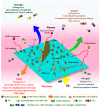
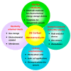
Schematic representations of possible applications of CNWs/other 2D carbon materials.

References

    1. Kroto H.W., Heath J.R., O’Brien S.C., Curl R.F., Smalley R.E. C60: Buckminsterfullerene. Nature. 1985;318:162. doi: 10.1038/318162a0. - DOI
    1. Ando Y., Zhao X., Ohkohchi M. Production of petal-like graphite sheets by hydrogen arc discharge. Carbon N. Y. 1997;35:153–158. doi: 10.1016/S0008-6223(96)00139-X. - DOI
    1. Wu Y., Qiao P., Chong T., Shen Z. Carbon nanowalls grown by microwave plasma enhanced chemical vapor deposition. Adv. Mater. 2002;14:64–67. doi: 10.1002/1521-4095(20020104)14:1<64::AID-ADMA64>3.0.CO;2-G. - DOI
    1. Novoselov K.S., Geim A.K., Morozov S.V., Jiang D., Zhang Y., Dubonos S.V., Grigorieva I.V., Firsov A.A. Electric field in atomically thin carbon films. Science. 2004 doi: 10.1126/science.1102896. - DOI - PubMed
    1. Machino T., Takeuchi W., Kano H., Hiramatsu M., Hori M. Synthesis of platinum nanoparticles on two-dimensional carbon nanostructures with an ultrahigh aspect ratio employing supercritical fluid chemical vapor deposition process. Appl. Phys. Express. 2009;2:025001. doi: 10.1143/APEX.2.025001. - DOI

LinkOut - more resources