. 2019 Mar 5;116(10):3968-3973.
doi: 10.1073/pnas.1813001116. Epub 2019 Feb 12.

From 2D to 3D: Strain- and elongation-free topological transformations of optoelectronic circuits

Affiliations

From 2D to 3D: Strain- and elongation-free topological transformations of optoelectronic circuits

Dejiu Fan et al. Proc Natl Acad Sci U S A. .

Abstract

Optoelectronic circuits in 3D shapes with large deformations can offer additional functionalities inaccessible to conventional planar electronics based on 2D geometries constrained by conventional photolithographic patterning processes. A light-sensing focal plane array (FPA) used in imagers is one example of a system that can benefit from fabrication on curved surfaces. By mimicking the hemispherical shape of the retina in the human eye, a hemispherical FPA provides a low-aberration image with a wide field of view. Due to the inherently high value of such applications, intensive efforts have been devoted to solving the problem of transforming a circuit fabricated on a flat wafer surface to an arbitrary shape without loss of performance or distorting the linear layouts that are the natural product of this fabrication paradigm. Here we report a general approach for fabricating electronic circuits and optoelectronic devices on nondevelopable surfaces by introducing shear slip of thin-film circuit components relative to the distorting substrate. In particular, we demonstrate retina-like imagers that allow for a topological transformation from a plane to a hemisphere without changing the relative positions of the pixels from that initially laid out on a planar surface. As a result, the resolution of the imager, particularly in the foveal region, is not compromised by stretching or creasing that inevitably results in transforming a 2D plane into a 3D geometry. The demonstration provides a general strategy for realizing high-density integrated circuits on randomly shaped, nondevelopable surfaces.

Keywords: semiconductor processing; sensor arrays; topological transformation.


Conflict of interest statement

Conflict of interest statement: Several intellectual property disclosures have been submitted to the University of Michigan’s Office of Technology Transfer over the years that this work was carried out. Several of these disclosures have resulted in provisional and US utility patents. No license agreements have been established with third parties.

Figures
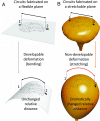
Fig. 1.
Fig. 1.
Schematic illustration of a developable deformation vs. nondevelopable deformation process. (A) Circuits fabricated on a flexible plane and deformed into a developable semicylindrical shape that does not entail a topological transformation. The distance between points 1 and 2 along the surface remains the same after the deformation. (B) Circuits fabricated on a stretchable plane (a deflated balloon) and deformed into a nondevelopable, topologically distinct spherical shape (an inflated balloon). The distance between points 1 and 2 along the surface is dramatically increased after the deformation.
Fig. 2.
Fig. 2.
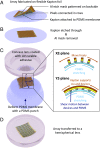
Schematic illustration of the key steps of fabricating a hemispherical photodiode array. (A) GaAs p-n junction photodiode array connected in rows fabricated on flexible Kapton substrate (brown) with an Al etch mask (light gray) patterned on the backside, is laid flat onto a poly(dimethylsiloxane) (PDMS) membrane (purple). (B) The Kapton substrate is etched through to the PDMS surface using O2 plasma. The Al etch mask is removed using Cl2 plasma. (C) The PDMS membrane that supports the array is fixed on its edges and deformed by a centered PDMS hemispherical punch. The array is transferred to a matching hemispherical concave glass lens coated with UV curable adhesive. (C, Inset) Cross-section views from the xz plane and the xy plane during the deformation process. Kapton substrate (brown) supports Au connection lines (yellow) and photodiode mesas (gray) when the PDMS membrane (blue) is stretched. Rows of pixels are free to move in the x direction and have shear motion with the PDMS membrane in the y direction. (D) Array (connected in rows) transferred to the concave glass lens.
Fig. 3.
Fig. 3.
(A) Photograph of a 15 × 15-pixel GaAs p-n junction photodiode array fabricated on a concave hemispherical surface. Additional 4 × 2 peripheral pixels that allow for motion detection at wide angles of view are also shown. (B) Scanning electron microscopic image of a portion of the photodiode array. (C) Schematic of a single pixel in the array. (D) External quantum efficiency (EQE) spectra of the photodiode in the wavelength range from 400 nm to 900 nm. (D, Inset) Current-voltage (I-V) characteristics of the photodiode in the dark (blue line) and under 64-nW, 530-nm light-emitting diode (LED) illumination (orange line). (E) Histogram of dark current of photodiodes on the 15 × 15 FPA. (E, Inset) Normalized dark current maps of the 15 × 15 GaAs FPA on the hemispherical surface. (F) Photocurrent vs. input optical power of a single photodetector in the 15 × 15 FPA. Red line shows a linear fit to the photocurrent at low-input optical power. The minimum detectable power is about 10−4 W/cm2, and the 1-dB compression point is at 0.1 W/cm2, giving a 30-dB dynamic range and a 10-bit grayscale resolution.
Fig. 4.
Fig. 4.
(A) Ray-tracing simulation result of an object (3 cm wide) located 10 cm from a plano-convex lens (black contour). Rays from the object are focused by the lens onto the FPA surface (orange curve, 3.0 cm from the lens). (B) Magnified view around the hemispherical imager (black contour). The simulated lens focal surface (blue dashed line) has good overlap with the concave FPA surface (front curve of the black contour). (C) Photograph of the hemispherical FPA mounted on a 3D-printed substrate holder integrated with a 3D-printed lens holder. Also presented is a 48-channel probe card used to read currents generated by all pixels on the hemispherical FPA simultaneously. (D) Side view of the experimental setup for imaging acquisition. (E) Normalized photocurrent map on the 15 × 15 FPA showing images of letters “O,” “C,” and “M.” A leakage current threshold of 15.8 nA is applied to minimize obscuration of the images by the background sneak currents.

Comment in

  • QnAs with Stephen R. Forrest.
    Ahmed F. Ahmed F. Proc Natl Acad Sci U S A. 2019 May 7;116(19):9147-9148. doi: 10.1073/pnas.1903867116. Epub 2019 Apr 22. Proc Natl Acad Sci U S A. 2019. PMID: 31010923 Free PMC article. No abstract available.

References

    1. Guenter B, et al. Highly curved image sensors: A practical approach for improved optical performance. Opt Express. 2017;25:13010–13023. - PubMed
    1. Dinyari R, Rim S-B, Huang K, Catrysse PB, Peumans P. Curving monolithic silicon for nonplanar focal plane array applications. Appl Phys Lett. 2008;92:091114.
    1. Rim S-B, Catrysse PB, Dinyari R, Huang K, Peumans P. The optical advantages of curved focal plane arrays. Opt Express. 2008;16:4965–4971. - PubMed
    1. Fan D, Lee K, Forrest SR. Flexible thin-film InGaAs photodiode focal plane array. ACS Photonics. 2016;3:670–676.
    1. Ko HC, et al. A hemispherical electronic eye camera based on compressible silicon optoelectronics. Nature. 2008;454:748–753. - PubMed

Publication types