Review
. 2019 Jan 4;7(1):1800419.
doi: 10.1002/adom.201800419. Epub 2018 Sep 16.

Additive Manufacturing: Applications and Directions in Photonics and Optoelectronics

Affiliations
Review

Additive Manufacturing: Applications and Directions in Photonics and Optoelectronics

Andrea Camposeo et al. Adv Opt Mater. .

Abstract

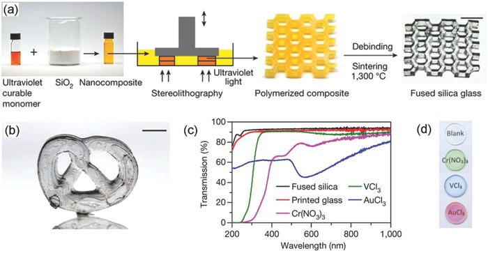
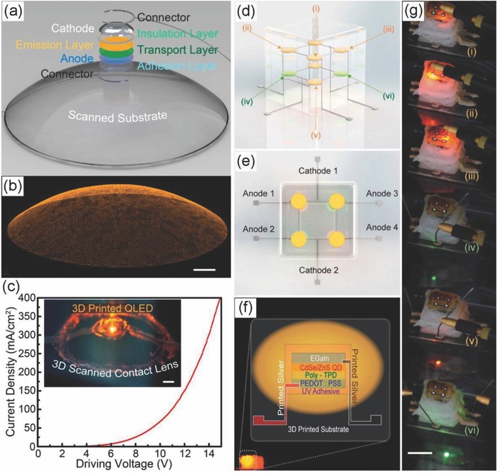
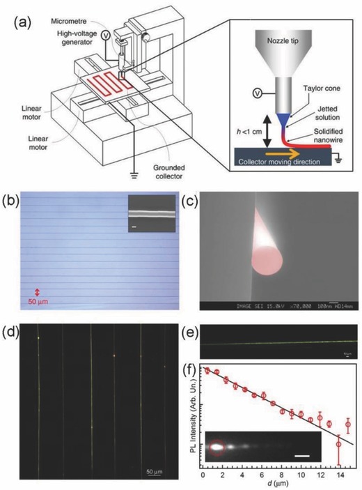
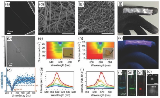
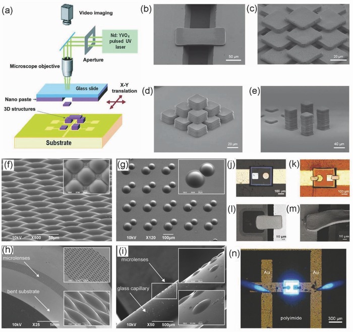
The combination of materials with targeted optical properties and of complex, 3D architectures, which can be nowadays obtained by additive manufacturing, opens unprecedented opportunities for developing new integrated systems in photonics and optoelectronics. The recent progress in additive technologies for processing optical materials is here presented, with emphasis on accessible geometries, achievable spatial resolution, and requirements for printable optical materials. Relevant examples of photonic and optoelectronic devices fabricated by 3D printing are shown, which include light-emitting diodes, lasers, waveguides, optical sensors, photonic crystals and metamaterials, and micro-optical components. The potential of additive manufacturing applied to photonics and optoelectronics is enormous, and the field is still in its infancy. Future directions for research include the development of fully printable optical and architected materials, of effective and versatile platforms for multimaterial processing, and of high-throughput 3D printing technologies that can concomitantly reach high resolution and large working volumes.

Keywords: 3D printing; additive manufacturing; direct ink writing; electrospinning; light‐emitting devices; optical sensors; waveguides.


Figures

Figure 1
Figure 1
3D printed transparent glass. a) Schematics of the printing process of fused silica glass: first amorphous silica powder is mixed with an UV‐curable monomer, and the resulting nanocomposite resin is patterned by STL. The polymerized material is then converted in fused silica glass through debinding and sintering thermal treatments. Scale bar: 7 mm. b) Example of a 3D‐printed and sintered glass structure. Scale bar: 5 mm. c) UV–visible transmission spectrum of printed and sintered glass (black continuous line). The spectrum of commercial fused silica is shown for comparison. d) Example of colored fused silica glasses obtained upon doping with metal salts. Reproduced with permission.43 Copyright 2017, Macmillan Publishers Limited.
Figure 2
Figure 2
DLP‐printed pH optical sensor. a) Scheme of 3D printing system used to fabricate the PAA microstructures on the surface of an optical tapered fiber. b) pH‐sensing device. c) Optical microscopy image of a tapered optical fiber with a diameter of 30 µm. The insets c1, c2, and c3 show confocal microscopy images of PAA micropads printed on the fiber, with sizes: 325 × 100 µm2 (c1), 325 × 300 µm2 (c2) and 325 × 600 µm2 (c3). Insets in (c1–c3): photo of the devices. d) Reversible shift of the wavelength of the optical transmission dip versus pH. The inset shows the transmission spectra of the printed device at various values of pH. e) Dynamic response of the printed optical sensor (i.e., wavelength shift, left vertical scale) to different pH solutions (right vertical scale). Reproduced with permission.46 Copyright 2016, Wiley‐VCH.
Figure 3
Figure 3
a) A photonic crystal and b) a complex concentric microstructure made using SZ2080. (a) Reproduced with permission.75 Copyright 2008, American Chemical Society. (b) Reproduced with permission.78 Copyright 2015, American Vacuum Society. c–e) Freestanding lens compound optical systems: (c) device schemes, (d) simulated images by using a USAF 1951 resolution test chart, (e) actual devices; scale bars: 20 µm. (c–e) Reproduced with permission.79 Copyright 2016, Macmillan Publishers Limited. f–i) A system of four different compound lenses on the same CMOS image sensor, combining different fields of view in one single system: (f) device schemes, (g) corresponding pixel size, evidencing an increased resolution toward the center of the image, (h, i) actual devices printed by MP‐STL. (f–i) Reproduced under the terms of the CC‐BY‐NC license.22 Copyright 2017, The Authors, some rights reserved; exclusive licensee American Association for the Advancement of Science.
Figure 4
Figure 4
a) A complex lens system on the end of an optical fiber. Scale bar: 25 µm. Reproduced under the terms of the CC‐BY license.82 Copyright 2016, The Authors. Published by Macmillan Publishers Limited. b) A fiber‐end Fabry–Perot gas microsensor, built directly on the top of a fiber. Reproduced with permission.86 Copyright 2015, IEEE. c–g) Examples of 3D metamaterial structures made using MP‐STL and selective electroless plating. (c)–(f) Reproduced with permission.98 Copyright 2017, Wiley‐VCH. (g) Reproduced with permission.99 Copyright 2015, American Chemical Society.
Figure 5
Figure 5
Material and process properties in DIW. a) Storage shear modulus, G′, versus applied shear stress for a fugitive ink filled with nanoparticles (fill circles) and for an organic ink doped with 40 wt% of microcrystalline wax (empty circles). The insets show optical images of corresponding suspended filaments (length 10 mm and diameter about 1 mm), acquired 1 h after printing. Reproduced with permission.116 Copyright 2005, Wiley‐VCH. b) Viscosity versus shear rate for two inks with 20 wt% (circles) and 23 wt% (squares) of silica nanoparticles. The photographs show the corresponding printed samples which have very different optical transparency. Low silica content favors fusion of printed filaments (left pictures), whereas increasing silica content allows stable gap‐spanning features, but leads to lower optical transparency (right pictures). Scale bar: 4 mm. Inset scale bar: 0.5 mm. Reproduced with permission.117 Copyright 2017, Wiley‐VCH. c) Schematic representation of a typical setup for 3D printing by DIW. d) Images of elementary structures printed by DIW for various process parameters, H* and V*, corresponding to the diverse printing modes. (c), (d) Reproduced with permission.115 Copyright 2018, Wiley‐VCH.
Figure 6
Figure 6
Waveguides printed by DIW. a) Optical microscopy image of printed silk waveguides. b) Higher magnification optical microscopy image of the curved region of the silk waveguide, as highlighted by a dashed box in (a). Inset: SEM image of the printed silk waveguide. c) Cross‐sectional optical image of a cleaved silk waveguide. d,e) Photographs showing diffused laser light coupled in straight (d) and curved (e) silk waveguides. f) Cross‐sectional view of light diffused by the cleaved surface of a silk waveguide. (a)–(f) Reproduced with permission.122 Copyright 2009, Wiley‐VCH. g) Photograph of curved waveguides made of OrmoClear. h) Optical propagation losses versus the radius of curvature of the waveguides. i) Photograph of a network of six OrmoClear waveguides with coupled LED light at three different colors. (g)–(i) Reproduced with permission.124 Copyright 2011, Wiley‐VCH.
Figure 7
Figure 7
Photonic crystals by DIW. a) Scheme of a woodpile photonic crystal structure printed by DIW. b) SEM image of a Si/SiO2/Si hollow woodpile structure, realized by c) the multistep method schematized. d) SEM image of an individual hollow filament of the Si/SiO2/Si photonic crystal. (a)–(d) Reproduced with permission.126 Copyright 2006, Wiley‐VCH. e) A BaTiO3/PDMS nanocomposite 3D photonic crystal upon bending. f) Scheme of the variation of photonic crystal morphology under elongational stress. g,h) SEM images of 3D nanocomposite photonic crystals as viewed from the top (g) and in cross‐section (h). i) Measured transmission terahertz spectra of 3D nanocomposite photonic crystals, realized by printing inks with various BaTiO3 content. j) Transmission terahertz spectra of the 3D nanocomposite photonic crystals upon varying the relative elongation as schematized in (f). (e)–(j) Reproduced with permission.127 Copyright 2017, Wiley‐VCH.
Figure 8
Figure 8
3D printed QD LEDs. a) 3D digital model of a QD LED to be printed on a curved substrate, whose scanned surface is shown in b). c) Current density versus the driving voltage of a QD LED printed on top of the surface of a contact lens. Inset: device image. Scale bar: 1 mm. d,e) Design of a 2 × 2 × 2 array of QD LEDs and of their electrical interconnects. f) Schematic illustration of the device architecture and of the layers of each QD LED component. g) Photographs of QD LED devices of the top layer (i)–(iii) and of the bottom layer (iv)–(vi). The letters (i)–(vi) highlight the assigned LED position in the 3D array, as illustrated in (d). Scale bar: 1 cm. Reproduced with permission.128 Copyright 2014, American Chemical Society.
Figure 9
Figure 9
Direct printing by ES. a) Schematic illustration of a typical setup used for printing by ES. b) Optical microscopy image of an array of parallel printed filaments made by poly(9‐vinyl carbazole) (PVK). Inset: SEM image of a PVK filament. Scale bar: 200 nm. c) Cross‐sectional view of a PVK fiber imaged by SEM. (a)–(c) Reproduced with permission.133 Copyright 2013, Macmillan Publishers Limited. d,e) Confocal fluorescence microscopy image of an array of parallel filaments (d) and of a single fiber (e) made of MEH‐PPV/PEO. f) Plot of the fluorescence intensity transported through a printed fiber waveguide versus the distance, d, from the excitation spot. The continuous line is a fit to the data by an exponential decay function. Inset: fluorescence microscopy image of a MEH‐PPV/PEO fiber. The red circle highlights the excitation focused laser. Scale bar: 2 µm. (d)–(f) Reproduced under the terms of the CC‐BY license.134 Copyright 2013, The Authors. Published by The Royal Society of Chemistry.
Figure 10
Figure 10
Examples of photonic devices made by ES. a) SEM image of a freestanding polymer waveguide doped with single QDs. b) Fluorescence image of a waveguide embedding an isolated QD, which is highlighted by a dashed box. c) Plot of the second order correlation function, g 2(t), measured by continuous wave laser excitation. The continuous line is a fit to the data by: g 2(t) ∼ 1 − (1/N)exp(|t|/τ), t is time and τ is the fluorescence decay time. The fit gives a value of g 2(t) = 0.1 at t = 0 delays, that is indicative of single photon emission. (a)–(c) Reproduced under the terms of the CC‐BY license.135 Copyright 2016, The Authors. Published by American Chemical Society. d–i) Examples of random laser devices. SEM images of an array of polycaprolactone (PCL) filaments (d) and of PCL filaments with silica nanoparticles deposited by biomineralization (g). Scale bars: 5 µm. The corresponding emission intensity maps and emission spectra, showing the variation of the photoluminescence as a function of the pumping fluence, are shown in (e), (f) and (h), (i), respectively. Insets in (e), (h): sample photographs. Scale bar: 5 mm. (d)–(i) Reproduced under the terms of the CC‐BY‐NC‐ND license.136 Copyright 2018, The Authors. Published by Wiley‐VCH. j) Bright light and k) UV‐excited emission photographs of an array of uniaxially aligned polymer filaments, doped with an UV dye. l–n) Photographs of emission from blue‐, green‐, and red‐emitting chromophores, respectively, in solutions excited by the UV light beam emitted by the array of polymer filaments. o) Images of the beam spot emitted by the polymer filaments at various distances, z, from the light source (top image: z = 0 mm, bottom image z = 1 mm). The beam divergence is 16.5 mrad. (j)–(o) Reproduced under the terms of the CC‐BY‐NC license.137 Copyright 2015, The Authors. Published by American Chemical Society.
Figure 11
Figure 11
3D optical waveguides. a) Schematics of the 3D printing process based on the stretching of the meniscus of a polymer solution. b) SEM image of a polystyrene 3D waveguide. Insets: zooms of the sample regions highlighted by the white and black box, respectively. c) SEM image of crossed 3D waveguides. The insets show magnified views of the crossing area. d,e) Examples of 3D waveguides printed through a gap (d) and a step (e). f) Schematic illustration of a 3D‐printed interconnect between ZnO nanorods. g) SEM image of a printed waveguide (P1) connecting two ZnO nanorods (Z1 and Z2) and h) corresponding fluorescence map, obtained by exciting the Z1 nanorod by a focused laser as schematized in (f). The fluorescence map evidences the optical coupling between Z1 and Z2 through P1, whereas no signal is observed from Z3. i) Schematics of a multibranched 3D optical interconnect. j) SEM image of a freestanding, multibranched, printed waveguide. The insets show a magnification of the branching point and of the area of coupling to nanoscale photon sources (NPSs), as highlighted by the white and black dashed boxes, respectively. Scale bars: 2 µm. Reproduced with permission.187 Copyright 2016, Wiley‐VCH.
Figure 12
Figure 12
Laser‐induced forward transfer of optoelectronic and micro‐optical components. a) Scheme of the experimental setup for 3D printing by LIFT. b–e) SEM of various structures realized by 3D printing of voxels composed by a silver paste, and assembled to form a bridge on a Si channel (width 100 µm) (b), a multilayer scaffold (c), a pyramid (d), and high‐aspect ratio pillars (e). (a)–(e) Reproduced with permission.193 Copyright 2010, Wiley‐VCH. f–i) Examples of arrays of microlenses manufactured by laser transfer. SEM images of an array of closed‐packed microlenses (f), of periodically arranged dimers of microlenses (g), and of an array of lenses printed on the surface of a bent substrate (h) and of a glass capillary (i). (f)–(i) Reproduced with permission.196 Copyright 2018, Wiley‐VCH. j,k) Images of a LED embedded in a polyimide substrate before (j) and after (k) printing of the interconnects. l,m) SEM images of the printed interconnects. n) Image of the manufactured LED under operation. (j)–(n) Reproduced with permission.193 Copyright 2010, Wiley‐VCH.
Figure 13
Figure 13
3D light‐emitting microparticles. a) Schematic diagram of a continuous flow lithography system, utilizing multiple coflows of monomers with lanthanide‐doped fluorescent nanoparticles. The inset shows fluorescence images of various manufactured particles. Reproduced with permission.203 Copyright 2014, Macmillan Publishers Limited. b) Schematics of two‐photon continuous lithography. c) Bright field optical microscopy image of a 3D helical particle made by two‐photon continuous flow lithography. d) The corresponding fluorescence microscopy image is shown. (b)–(d) Reproduced with permission.204 Copyright 2012, Wiley‐VCH. e) Fluorescent microparticles as encoded barcodes in anticounterfeiting. The imaging system utilized a portable detector (Apple iPhone 4S with a 20× objective), as shown in the left image. The particles were embedded in various objects as shown in the top panels (from left to right: blister packs, banknotes, credit cards, curved ceramic objects, artwork, and high‐temperature‐cast polystyrene objects). The middle and bottom panels show the corresponding acquired images upon excitation with a 980 nm laser (excitation power: 1W) and without laser excitation, respectively. Reproduced with permission.203 Copyright 2014, Macmillan Publishers Limited.

References

    1. ISO/ASTM Standard 52900 , Standard Terminology for Additive Manufacturing – General Principles – Part 1: Terminology, ISO/ASTM International, Switzerland: 2015.
    1. Bourell D. L., Annu. Rev. Mater. Res. 2016, 46, 1.
    1. Ligon S. C., Liska R., Stampfl J., Gurr M., Mülhaupt R., Chem. Rev. 2017, 117, 10212. - PMC - PubMed
    1. Martin J. H., Yahata B. D., Hundley J. M., Mayer J. A., Schaedler T. A., Pollock T. M., Nature 2017, 549, 365. - PubMed
    1. Hirt L., Reiser A., Spolenak R., Zambelli T., Adv. Mater. 2017, 29, 1604211. - PubMed

LinkOut - more resources